-
wireless ergodox because why not
I’ve done kind of a lot of keyboards at this point. I made two Atreus from a kit, modified one to be wireless, and then almost completely rebuilt it after stepping on it and crushing the case. Then I got into Ergodox, and built one of those from an ok kit from Input Club. Finally, I decided 40% boards are not really for me, so I made a compact wireless planck that didn’t work terribly well ergonomically.
So, I have a lot of boards, and they’re all of the microcontroller with matrix variety. They were all kits because I thought hand-wiring was a pain in the ass, and large PCBs tend to be expensive to have custom-made for a one off. But, time moves on and I’d heard about what’s called ‘hand wiring,’ where you don’t need a pcb to hold the switches. I got some plates for an ergodox from a european company for a steal, and bought switches from Mouser. Then, this fall happened, in which I was super busy with work and travel and so nothing got done.
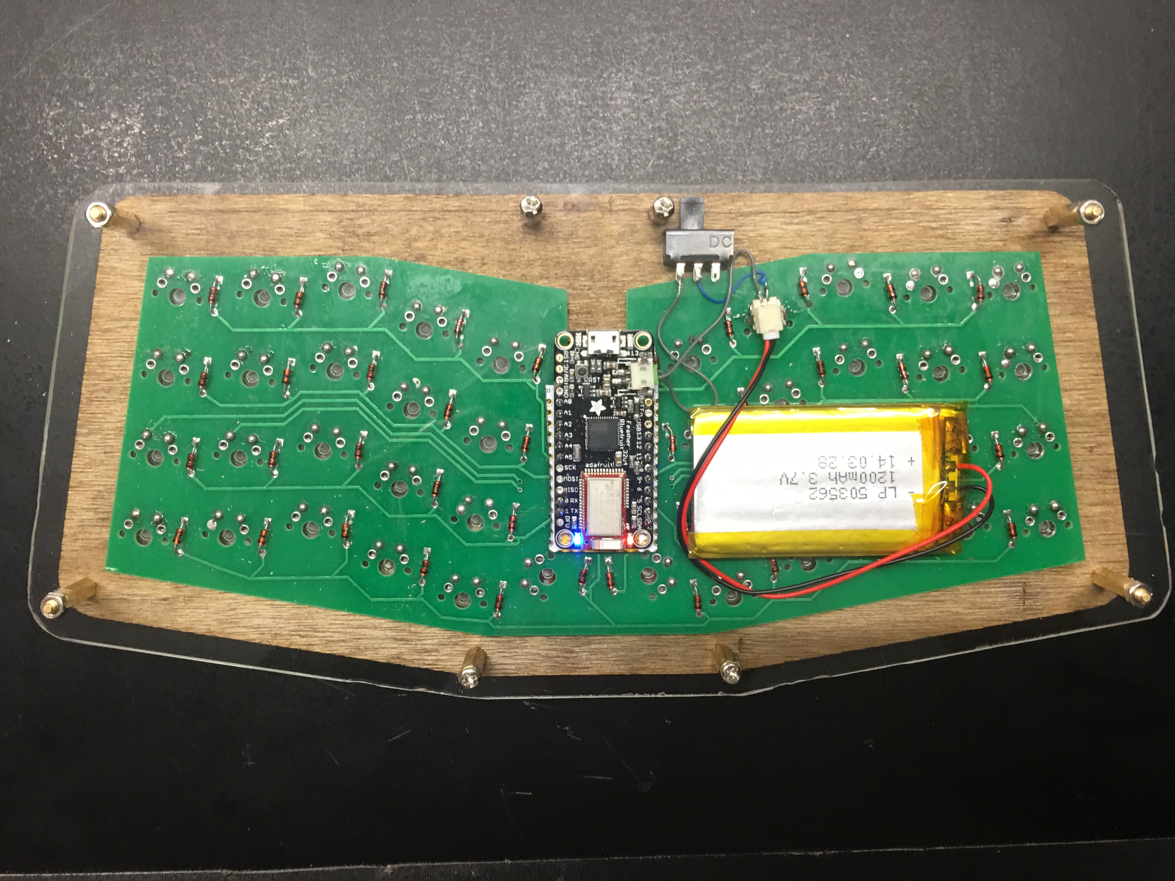
Thinking about it, though, that’s not true; I designed the thing and managed to solder all the components together before I went on vacation in October. I used an adafruit feather M0 w/bluetooth that I had sitting around, since they’re great for wireless keyboards, and the Boldport Ixpando, which is a breakout for the microchip MCP23017, a 16-bit i2c shift register. I read a couple guides on hand-wiring, bought a bunch of diodes, and threw it together. The bottom plates are some 3/16” aluminum I just happened to have laying around. Brass standoffs and M3 machine screws hold the key plates to the base.
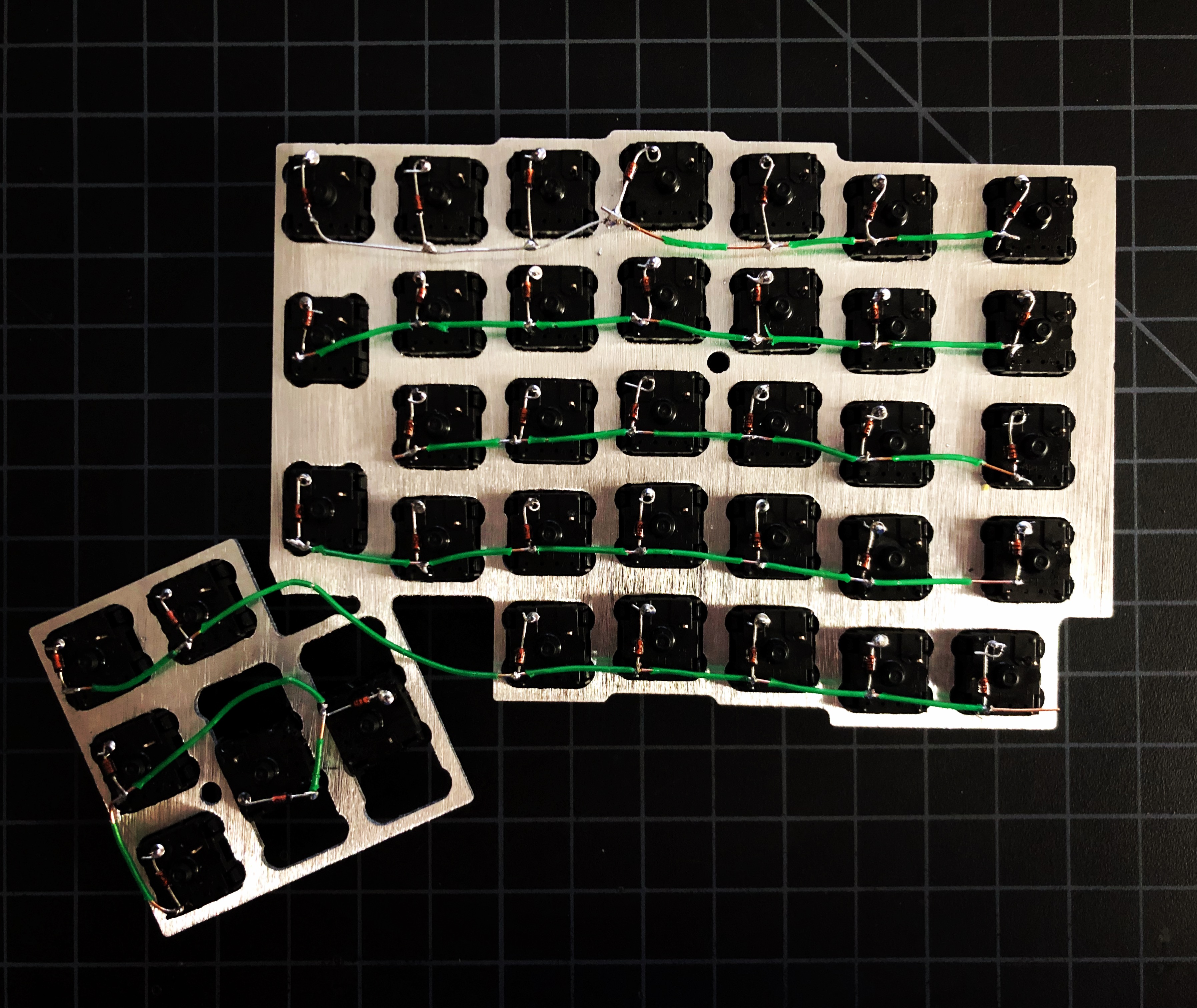
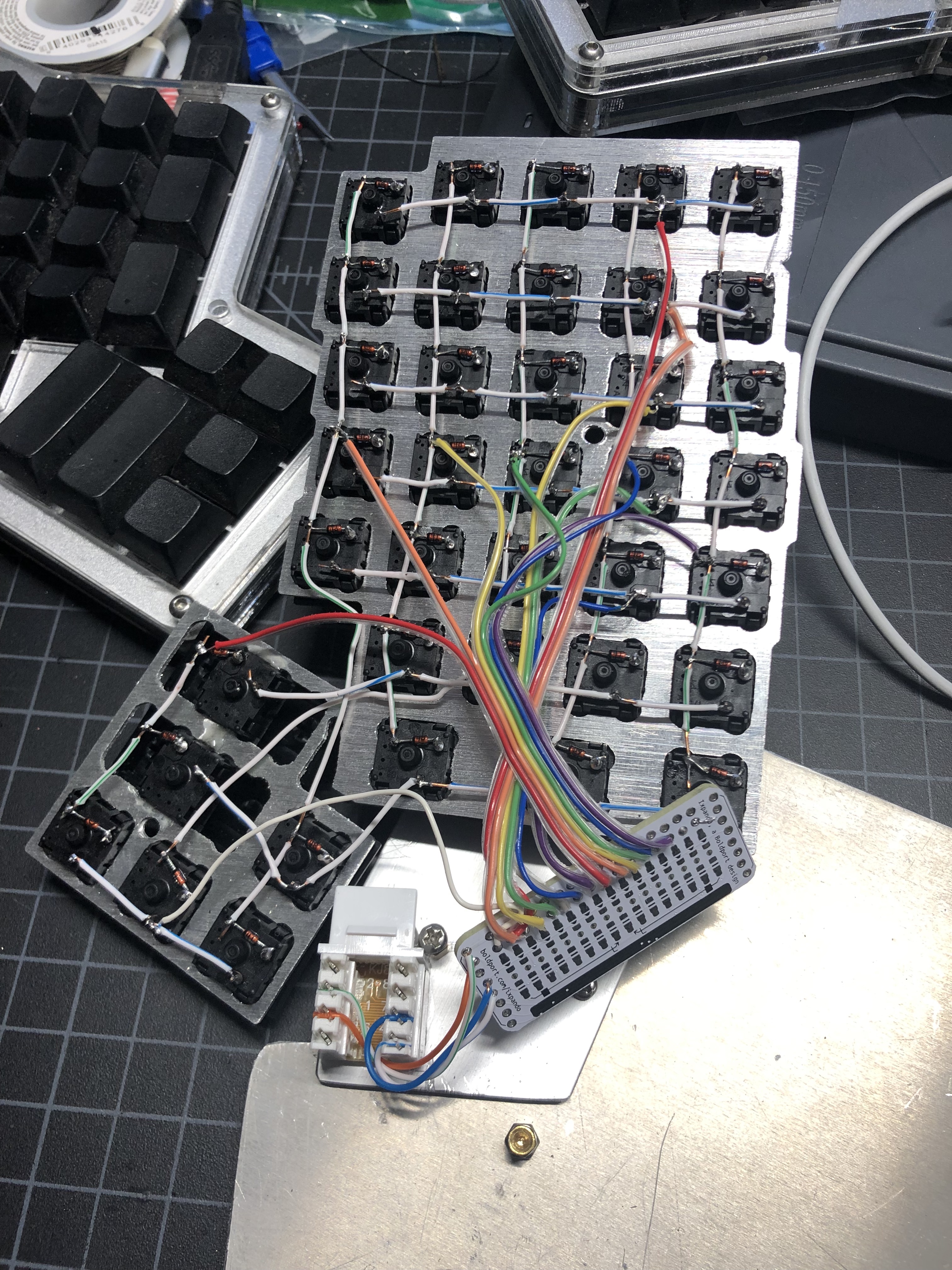
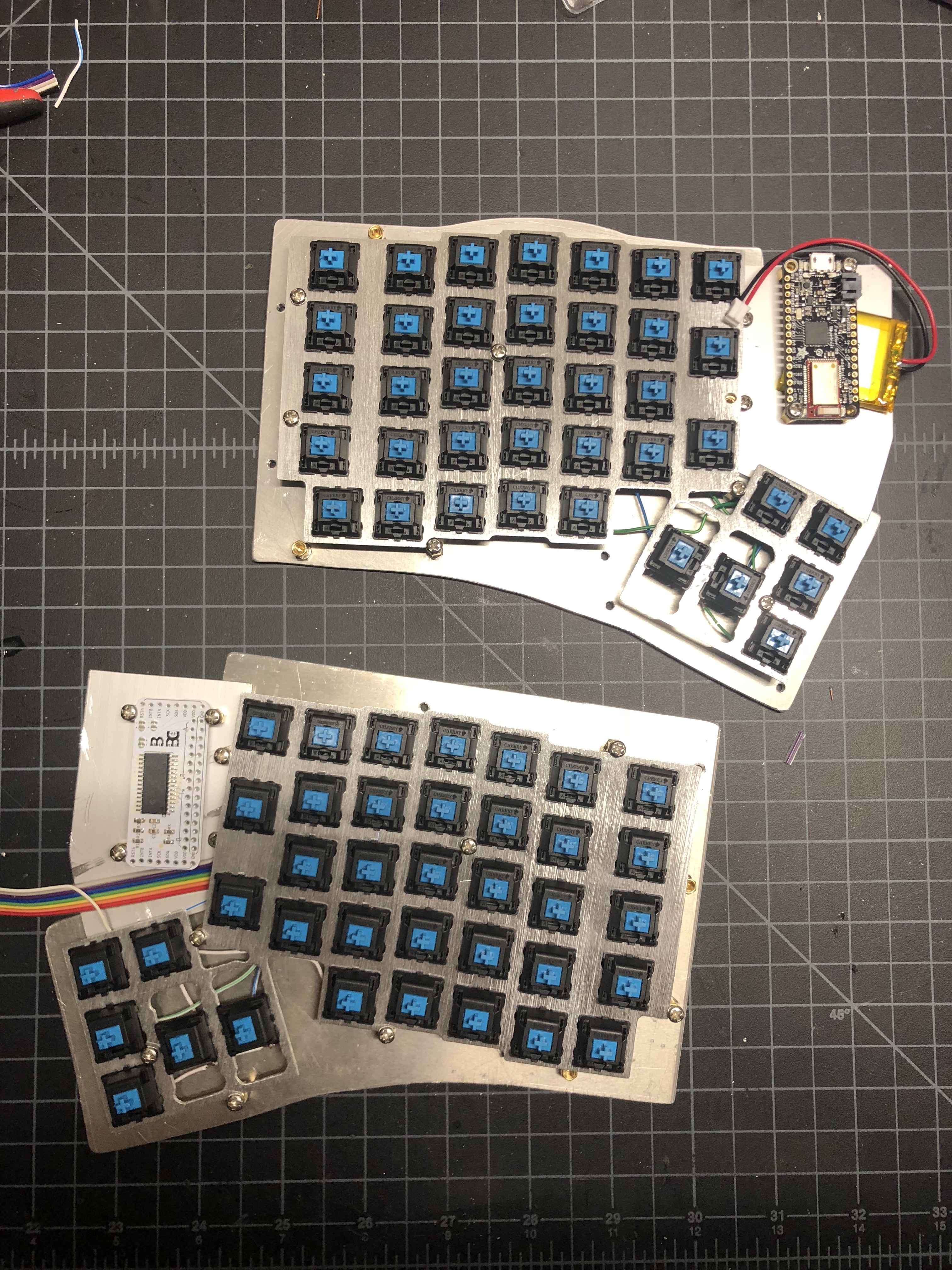
After I got that done, it sat for a couple months while other matters occupied my time. But, eventually I got back to it and modified my existing wireless keyboard firmware to work with the shift register. That’s a project that’s still ongoing, because there’s still a tiny bit of lag; 25ms to scan is a little too long. I’ve wrestled with it quite a bit just to get it to work, but it finally does.
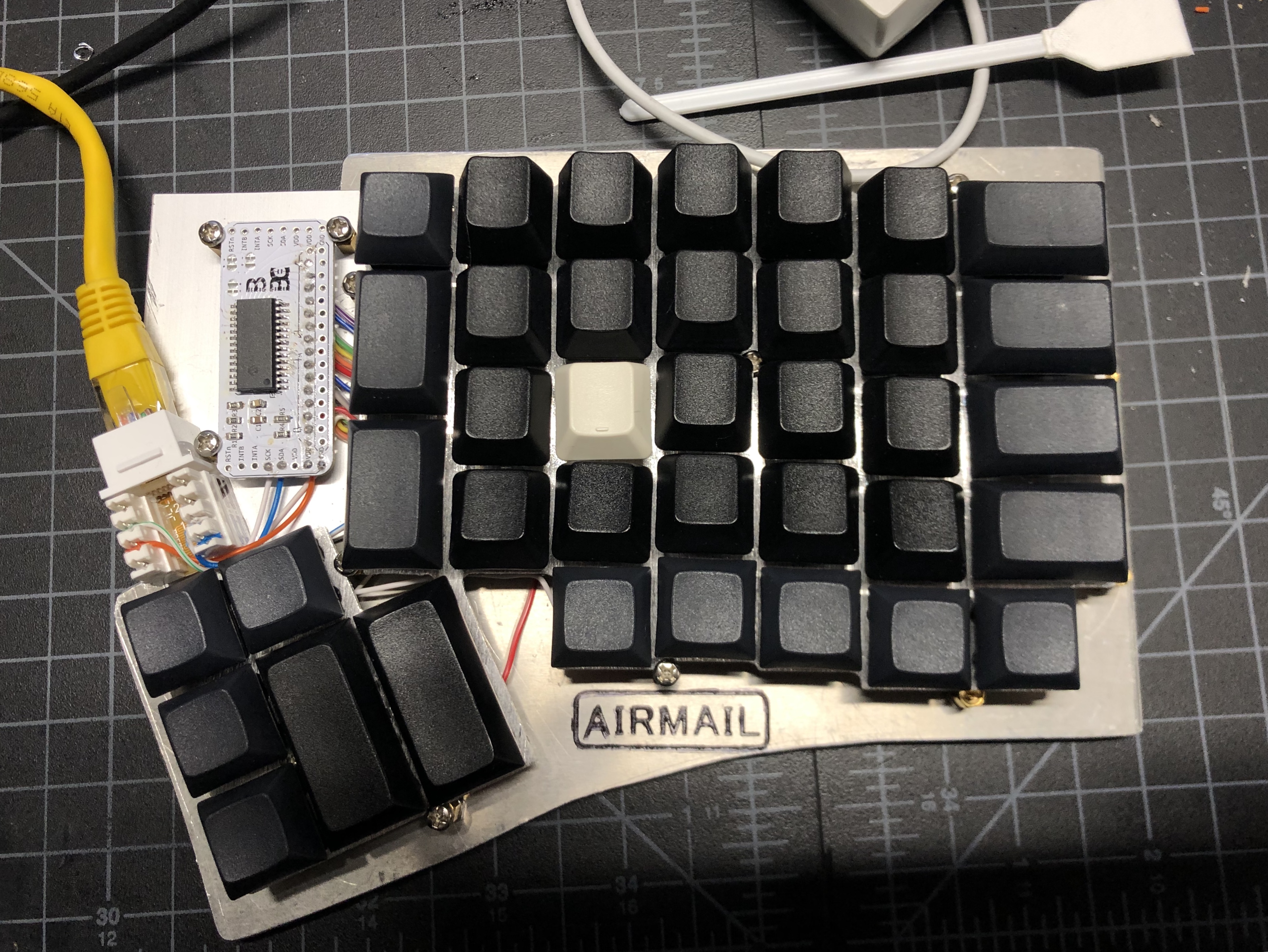

(If you look closely you can see that the battery is disconnected; that’s because I was debugging, but it works just fine. I do need to put in an on/off switch…)
-
iphone x
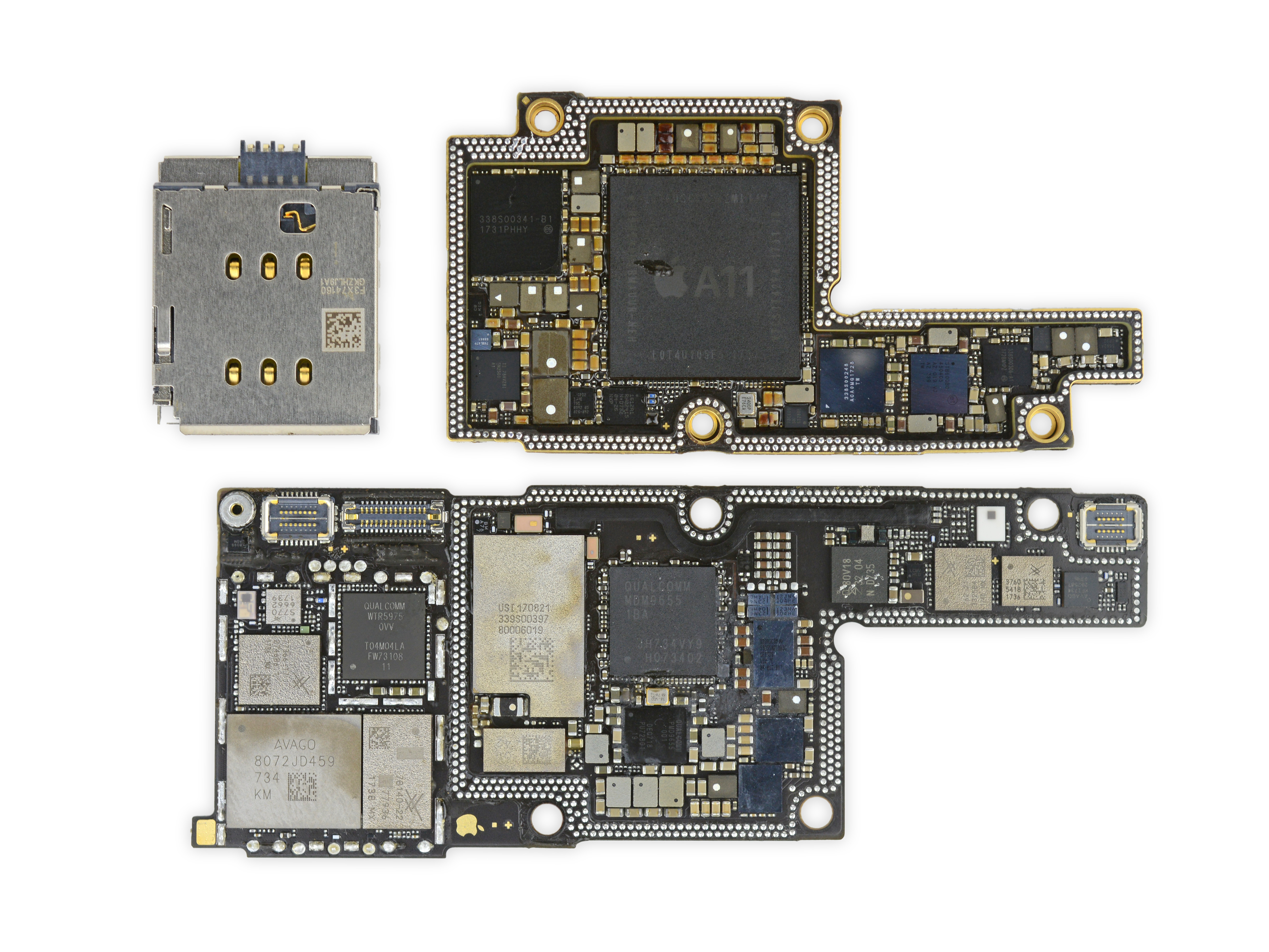
I just read the iFixit teardown of the new iPhone. The new phone is a remarkable piece of technology but I’d like to draw your attention to one image in that post:
Now, to most of you I’m sure this looks like a bunch of blobs and glitter, separated by large rectangles. It’s really a lot more than that though, and I’d like to talk about what I see when I look at this photo.
It’s a product shot, evenly lit, on a bright white background. The product stands in stark contrast to the cleanness of the surface it’s shot on. But other than that, it’s not much to write home about, aesthetically.
This picture is all about details, though. The surfaces of both sides of the interior of this PCB sandwich are a perfect horror vacui; every available space is covered. That means that almost none of the area on the top of the board is given over to traces, the lines on the board that actually connect the part; it also means there are a large number of blind and buried vias, which are both more expensive and error prone. I see this and I think, that’s gotta be at least an 8 layer board on each side.
Then I start to think about how I would design this. The upper bound for the number of traces, every pin discreetly connected to every other pin, is on the order of millions of them, but I’d be surprised if there were more than 10,000 “nets” (that is, discreet connections between sets of pins). For reference, my watch has 100, and took me a week to route. The engineers that built this board could do mine in an hour or two, probably; so we’re talking 1,000 engineer-hours just to route the connections on the boards. That’s one guy and 6 months, or a team of 10 (with managers) and 2 months (because engineering time doesn’t scale lineraly; coordination of effort takes time, too).
It’s probably a team of 20 and consistent 1 month iterations; they have to do quick turns for problems and changes in the supply chain, uncertainty about whatever parts come in, alternate versions for different vendors for different parts (different cellular radios, sensors, whatever). There’s a lot of uncertainty when you begin a project like this. You don’t know what the vendors can really deliver in 18 months in quantity 100 million. That’s not 20 engineers total, but 20 for this small facet of the overall design.
For example, the cameras. The cameras, even one of them but especially both of them, represent an amazing amount of work. The sensors had to go through design and testing; the optical systems, likewise. They have autofocus and optical image stabilization, which is completely nuts. Not just “man this is a lot of engineering” but “are we sure apple isn’t working with aliens on this one?” nuts. (It’s really just the progression of a bunch of related tech, including accelerometers and very small electromagnets, but I digress).
Even once you have that design, it’s not done; there are assembly and process engineers that have to do their work, too. The robots that place components work a certain way, and the tool paths that put the components in place have to be right, or there’ll be too many failures.
There are a couple other interesting facts I’ve gleaned from this picture: they’re using what look like chip antennas for bluetooth and WiFi, which is a little odd. I could be wrong about what those pink blobs are, though; usually the antenna is part of the metal bezel on the outside of the case (those may be test antennas or something, too). There’s the crazy notch in what turns out to be the bt/wifi chip to accommodate a big capacitor (first spotted on twitter by someone else). That either means the supplier put that there and they’re taking advantage of the board area, or apple asked them to make that notch. Nuts.
So, yeah. I might have to pick one up.
-
towards an open internet of things
Someone should go and invent an open standard and build a bunch of devices on it
— photomattmills (@photomattmills) September 20, 2017this reply of mine was kind of meant to be flippant, but it really got me thinking, what would it take to make a truly open IoT platform? What does that look like?
So first, and this is a thing Matt said as well: it needs to work without the internet. Manual controls, default modes, all need to be part and parcel of the thing. Like smartwatches: most of them don’t gracefully fail to ‘just a watch’ when you first have them and haven’t set them up, they just fail completely to do anything. Smart bulbs are another example: If I spend $60 on a smart bulb, it better turn on and respond to a fucking dimmer out of the box without an app. It’s not too much to ask; I know this because I’ve designed lightbulbs before.
So: let’s say you have the OpenHome app (terrible name, we’ll have to iterate on that), and you buy a light bulb that supports it. What does that setup look like? Ideally, you plug in the bulb, it turns on a bluetooth 4.0 radio and announces it’s there to the world; your app sees it and tells you there’s a new device, would you like to pair?
So, first: the device must work under all circumstances the dumb device worked. Second, service discovery and connection needs to be fairly seamless. once that’s done, the device needs to advertise what sensors and services it offers. If only we had an API for dynamically building APIs lying around… oh yeah, GraphQL.
So the first thing you query for is a list of supported things to adjust and sense, and make a UI that doesn’t suck for things like adjusting temperature and color and volume; and then just enable the sliders (come on, we know it’ll be some sliders) that the service supports. For our hypothetical light bulb, it could be on/off (boolean), brightness percentage (interger out of 100), and maybe color (RGB hex, so an INT). Our hypothetical app has default and customizable, sharable setups for all of these values. You also need to be able to group devices (turn off all the lightbulbs etc).
Ideally you’d have a little wall-wart server (remember those? what a joke in these days of raspberry pis and vocores &c) that you plugged in and actually all the new smart devices talked through it, so when you wanted to add a control device (tablet, phone, friend house sitting) it just joins the wifi, open the OpenHome app, it detects the OpenHome server (couple ways to do this), it asks you if you want to control all the things, and pings authorized users for ackles. Then, the same service discovery mechanism that works for one device will load the whole home into the newly minted authorized user’s device.
Will anybody implement this? Probably not.
-
laptop shenanigans
There is something wrong with me. Well, several things wrong with me, but I’m here to talk about laptops. Every couple years, I get tired of paying the apple tax, and get it into my head that I’m going to either
- Take some PC hardware and make it a hackintosh
- Make this year the year of linux on the desktop
So, for the last 9 months or so I’ve been screwing around, all the while my main machine was a pretty lackluster Macbook. It has times where it’ll just seize up suddenly. I’d had it maybe three months when I bought a Lenovo with the intention of turning it into a hackintosh, and when that didn’t work out, I tried to be an Ubuntu user for a month. That almost worked.
Eventually I gave up and committed to suffering with the macbook a little longer. There’s only so much of that I can take, though, so about a month ago I started again, in earnest. I figured I’d give a different distro a try, so I downloaded and installed Elementary on the Lenovo. It’s a really great desktop distro. Polishes a bunch of the rough edges of Ubuntu with a custom window manager, and some sensible defaults. No cruft at all, and runs really well.
It came down to a couple missing pieces of software though. The lightroom replacement, Darktable, well, it sucks. Like, its error conditions were difficult to troubleshoot for me, and I’m a developer. The UI is plain bad (sliders that are 4px on a side? who thought that was a good idea?). The methods for organizing photos are sub par. It’s possible it’s like KiCad and I’m a couple hours of video tutorials away from happy productivity, but I really doubt it. The aesthetic sense of the person who designed that UI… is just someone I’ll never understand. It’s like nobody told them it was supposed to look good, so they just threw all this junk in a bunch of different places.
Enough ranting about darktable, except to say that it’s actually gotten a little better in the last 2 years. Not a lot, someone needs to put some money into it and completely re-design the UI with a cohesive strategy, but a little. Slightly less crashy.
I did not, after that, try to find any 3d CAD software for linux. Blender is supposed to be usable, but it’s not really CAD, just 3D modeling.
So, I’m writing this from a 13” macbook pro, fresh out of the box this afternoon. it’s a thing of beauty. Everything works. I can use my 4k display at 4k. I can edit photos on that 4k display, and it’s marvelous. I’m reminded of basically every other tool I’ve used that’s suited for the job: it just gets out of the way. So yeah, I’m happy with the new machine.
-
the setup
Who are you, and what do you do?
I’m Matt Mills, I’m a programmer, a photographer, and maker of watches, among other things.
What hardware do you use?
For the programming, a Mac laptop, currently a 13” Macbook Pro, maxed out. This was an upgrade from the teeny macbook, and what a difference the horsepower makes. One of several ergonomic keyboards, and a 30” screen to plug it into on my desk. Programming happens mostly in my head, and the space between what I know and can find out with google.
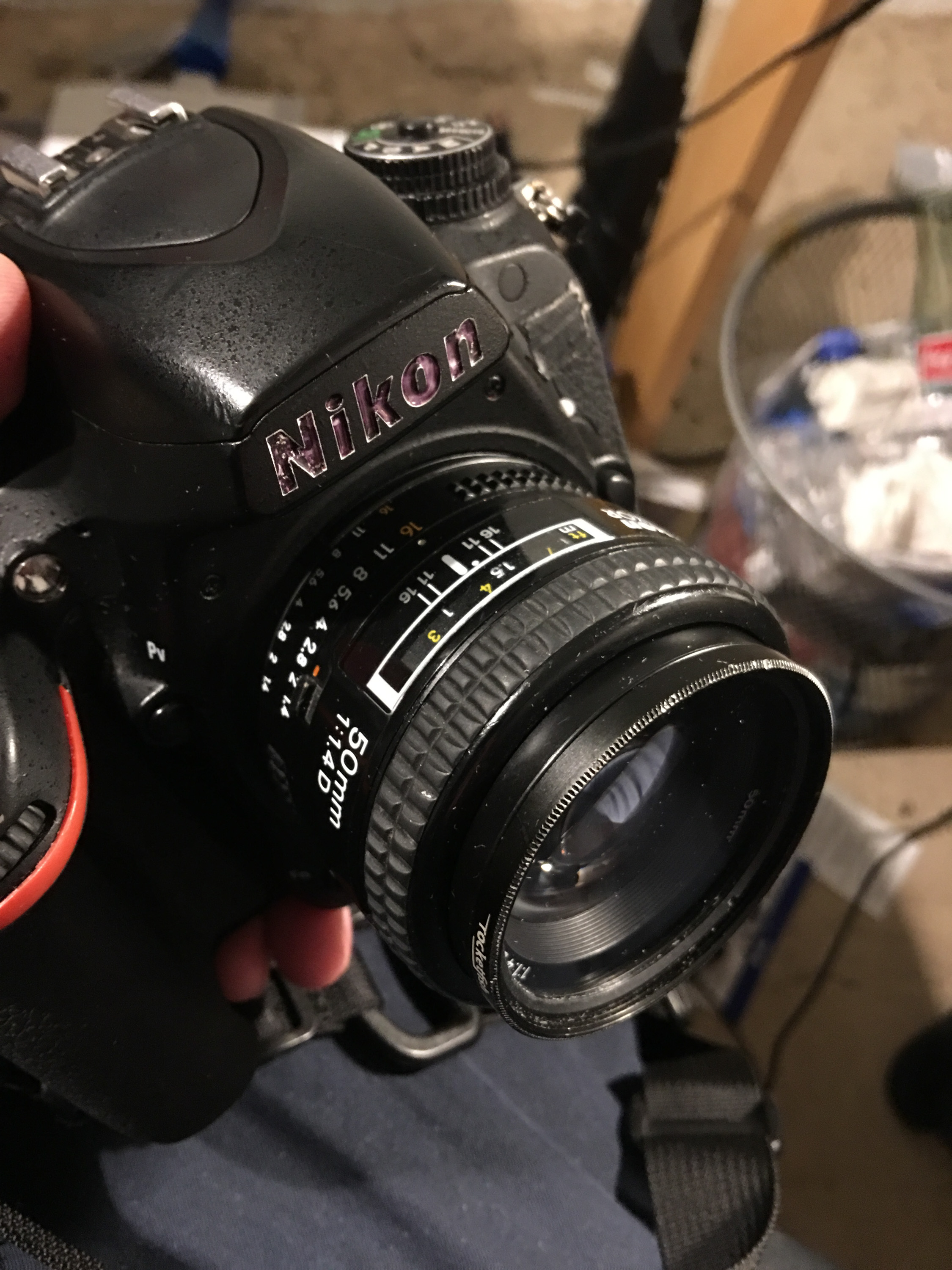
For the photography, I’ve got two main cameras, a Fuji XPro 2, and a Nikon D750. For lenses, I’ve got a 14mm f/2.8 and 35mm f/1.4 for the fuji, and a 24-120mm f/4, a 500mm f/6.3 mirror, a 40mm f/2, and a 50mm f1.4/D for the Nikon. I also have a bunch of 35mm cameras I never use, and some medium format gear, notably a Fuji GW690 II. Epson V600 scanner and P600 printer (which I hadn’t noticed until just now they’re the same number).
Like most photographers I know, I have a bag problem. Can’t find the perfect one, just keep trying. I used to really favor Domkes, but lately I’ve been carrying a ThinkTank Retrospective 7. It holds the laptop, and whatever camera setup I’m hauling currently. I also use a home-made messenger bag that’s sort of an amalgam of the different bags I’ve had and liked. Enough volume for an extra layer, tools, or a light grocery run, along with camera and laptop. Waterproofed with sailcloth, which is light and very durable.
For the making, too many hand tools to list, so maybe just my favorites? Knipex cutters, which are harder than nails at the business end. Not an expression: I’ve actually used them to cut framing nails. A Pfaff sewing machine that’s as old as I am, with “Made in West Germany” written on the front. A Printrbot simple metal, which I mostly just use to make watch cases. A hot-air reflow station, which makes so much possible when making and fixing circuits. Mitutoyo calipers; don’t skimp on your test equipment, since errors multiply each other.
Phone is an iPhone 6s+, in one of the thinner Otterbox cases. I go through cases about 1 per 6 months. This one might make it till the Fall. My EDC: phone, keys (with mini multitool, flashlight, Yubikey, and thumbdrive), a yellow benchmade griptilian, Pen Type B, and my wallet.
And what software?
On the desktop, it’s OSX with a ton of apps. Lightroom and Photoshop for photos, and if I’m working on images from the digital cameras, there’s never a reason to open photoshop. I’m typing this in Atom, the text editor from Github. It’s not the most amazing editor ever, but it works, and there are extensions for most of what I need; that’s for writing and coding. Tweetbot for twitter lists; I use private lists to make sense of the ~400 or so people I follow. I don’t try to get it all, except the friends list. Dropbox, although I don’t use it as much as I used to. Alfred, with the powerpack. Divvy, for fast window resizing. 1Password to keep me a little safer. Fusion 360 for CAD needs, except for electronics; all my circuits happen in KiCad.
On the phone, it’s Kindle, Signal, Tweetbot, Instagram, Dark Sky, and Google Maps. Other apps as needed (hi Terminus).
What would be your dream setup?
Something as small and thin as the macbook, with a quad core i7 and ALL THE RAM. A full machine shop, with a big mill and engine lathe and a chest full of bits and cutters, and a pile of stock in various flavors. A pair of Leica M10s, with 21mm and 50mm lenses on the front, and a Leica S for when I wanted medium format.
Enough money to pay off my student loans, and to give me time to take on freelance clients. I don’t need a fortune, although I wouldn’t say no if one was on offer.
-
the cost of freelancing (why I don't do it)
So, I was having a conversation on twitter about the economics of freelancing, and it occurred to me that a lot of my peers had no idea what the overhead of employing someone actually was. The business shorthand is that employing someone usually costs double their salary per annum; a little less for higher salary workers (they don’t use any more toilet paper than other workers, but tend to need specialized tools and environments to do their work, so it evens out). So, here’s a list of basic annual costs for a tech worker, with notes:
- Laptop ($1500 amortized over a 3 year life) - $500
- Monitor ($700 over 3 yr) - $233
- Office space - This is a little thornier; in SF it can be as much as $75/sq ft; in the midwest, more like $5/sq ft. $500/month for the space in a shared office seems reasonable – $6000
- Advertising, self-promotion, lead generation – $10000/yr (seems like a lot, but isn’t really)
- Health insurance – $600/mo*12 $7200/yr
- Internet (home/work) – $1200/yr
- Office furniture – (again amortized over 3 years; chairs, desk, lamp, etc; has to look good for client meetings): $2000
- Continuing education – Books, conferences, classes – $5000 (this is a low number; could easily double or triple)
- Phone (have to keep up with the joneses, and yes this is a business expense) – $1000
So, we’re already at $33,133. And we haven’t eaten anything for the year yet. You could cut some of these corners and maybe lose 20-30%, but just to push this above the poverty line, you have to make at least $60,000 in a year, in a place that’s fairly cheap to live. This is for a salary equivalent of $27k.
If we want to be a little more comfortable, a salary more in the $70k range would be good for someone in the midwest, in a decent sized city. Not “live in a fancy neighborhood with a family” nice, but suburbs with a family is maybe doable on that (don’t @ me, I know that’s not a lot of money for a family of four, but I know single moms that make a little less than that work). So that’s ~100k gross revenue with 2000 workable hours in a year (that’s 50 40 hour weeks and two for vacation) comes out to $50 per hour, right? Nope, because of utilization. In order to make $50/hr work, the contractor has to work all 2000 hours that year, which never happens. 50% of the time is a good ballpark number, although there are good years and bad years. Which brings us to $100/hr, which is still a really low rate, going from what I know people charge; there are a lot of other costs involved, and the market is pretty fierce. I know what I’d have to charge to make my salary and all those costs here in Oakland, and it’s more than double that.
There are other compounding factors; I haven’t mentioned the accounting and tax preparation overhead, in both time and money spent. Nor have I mentioned the business development aspects that can’t be neglected if you want to stay in business for more than a little bit. There’s also the opportunity cost of doing business in a place that’s not a big market for your skills; you can end up spending a lot on travel and expenses just to land clients that way (which is why the 10k number up there might be wildly low; also none of that is billable). Sometimes, clients just don’t pay after work has been delivered; that’s also a cost of doing business, and going after them costs more.
That’s not to say that it’s not doable. Many people enjoy the freelance hustle and flow. I’ve considered it myself, sometimes. But then I start to do some accounting like the above, and decide a salary isn’t so bad.
-
wireless atreus with Adafruit Feather
This is a project that I’ve been pecking away at, a little at a time, for something like a year and a half. I knew it was possible, from the data sheets and example code. It just took me a long time to take the idea and make it into a reality. For context, I’m typing this on the finished board, and it works just as well as the stock Atreus.
The first step to making this was to rip out the micro from my wired atreus. If you’re starting this from scratch, you may be able to do it cheaper, since there’s not much to recommend a PCB build over a hand-wired build. I did the kit at first because I didn’t have time to put the effort into figuring out everything I needed to build this by hand, and by the time I decided to make it wireless, I already had all the parts on hand. That said, here’s our bill of materials:
- One Adafruit Feather 32u, with bluetooth
- One Perma-Proto or generic perfboard
- one Atreus kit OR the list of keyboard parts
- wire
- solder
Keyboard parts (only needed if you don’t already have an atreus):
- 42 cherry key switches, panel mount in your preferred tactility. I like the blues, myself.
- 42 signal diodes, such as these
- a mounting plate, which can be made by Ponoko or similar. Or 3d printed, if you have a big enough printer.
- more wire
The hand-wiring of a keyboard is beyond the scope of this post, and there are many good tutorials and videos of it.
With the materials in hand, all that’s left is a bit of creative soldering. The idea is to use the perf board as an adapter. So, first, I soldered in some header at the right places to mate with the atreus’ holes. Luckily everything is on 0.1” headers, we just have to deal with a little offset. There are three pins we can’t use on the Feather, they’re the ones marked SCK, MOSI, and MISO. They’re required for the bluetooth part of the operation.
You can see in the pictures how I’ve connected the feather to the header, and added some jumper wires to make everything work. It’s simple enough that I didn’t even bother doing a circuit diagram. A0-A5 line up with the shorter side, and the long side gets three jumper wires to pins 1, 2, and 3. If you’re hand wiring, you won’t need the adapter board, just solder each row and column to its own IO pin.
I had to cut a hole in the top of my atreus’ switch plate, in order to get to the solder holes, but if you’re assembling from scratch with the kit, you should do all this before you put the switches in, and then solder the adapter/feather assembly into the main PCB.
I also did a little modification to the feather: I switched out the JST connector for a micro-sized one that I had laying around. This allowed me to get away with slightly less height for the overall keyboard.
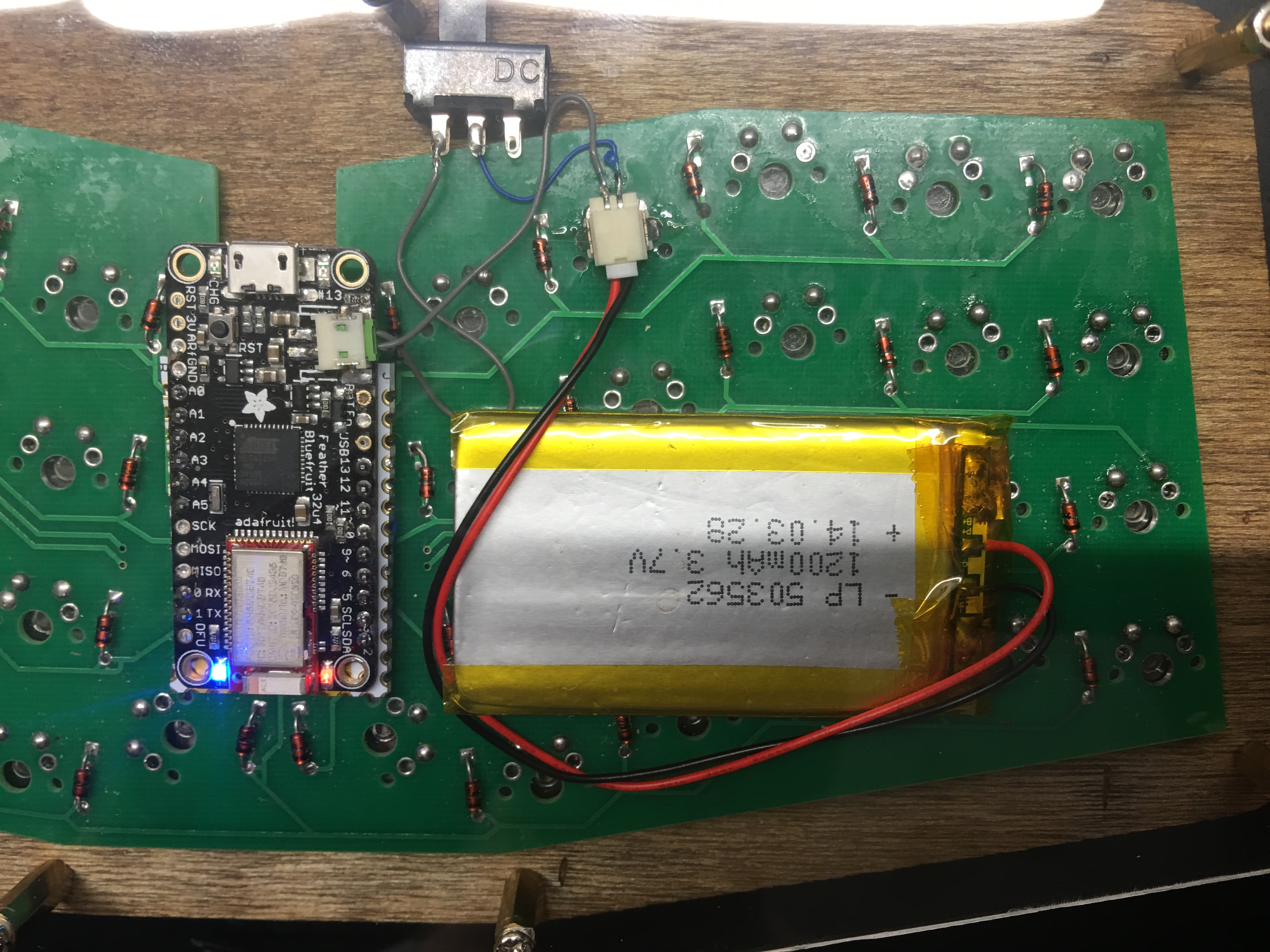
Then, I added a toggle switch to the ground line coming from the battery, hooked that and the positive terminal up to another connector, and plugged in the battery. I used some of the exposed pads to anchor the last connector; the mechanical connections are not electrically connected, so it works out. I could have made my life slightly simpler by soldering wires directly to the board, but I hadn’t worked out the entire strategy in advance; originally, I was going to just connect the battery to the micro-connector.
Once all that is done, and you have key the switches in, the firmware I’m using is here. It depends on the host OS for debounce; I haven’t had any issues yet on macOS, but YMMV, naturally. It’s otherwise kind of sloppy and in need of cleanup, but it works. The other thing is that there’s currently no third layer. Adding one would be pretty simple, but in practice I don’t need more than 84 keys (my ideal might be an atreus 64, actually).
This project is sort of a starting point from which I’d like to do a couple more keyboards. There’s this, and there’s the wireless ergodox build I’ve had on the back burner for quite a while, and maybe an atreus64 now that I know they exist.
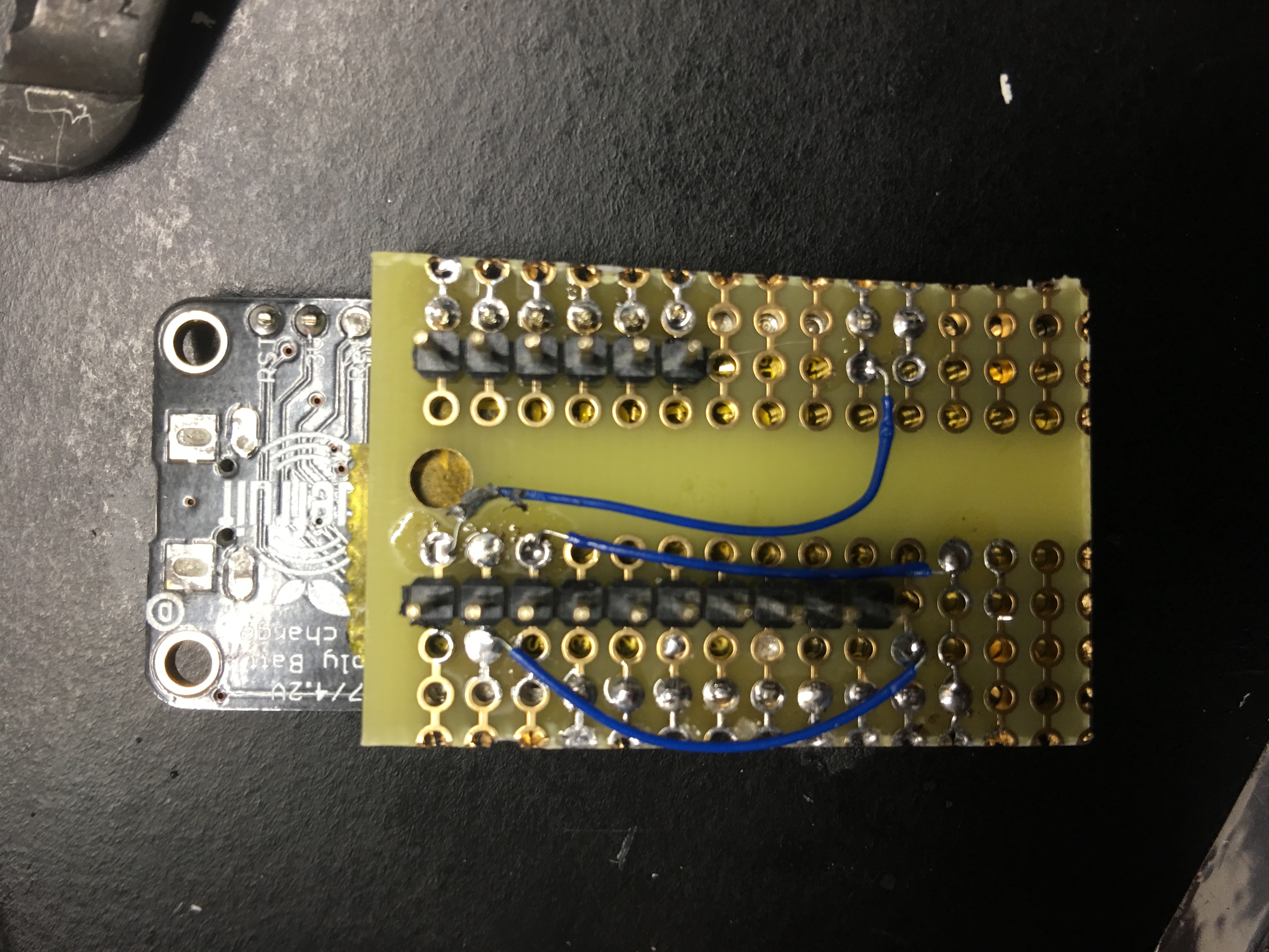 Illustration of my wiring. 30ga wire wrap wire to the rescue.
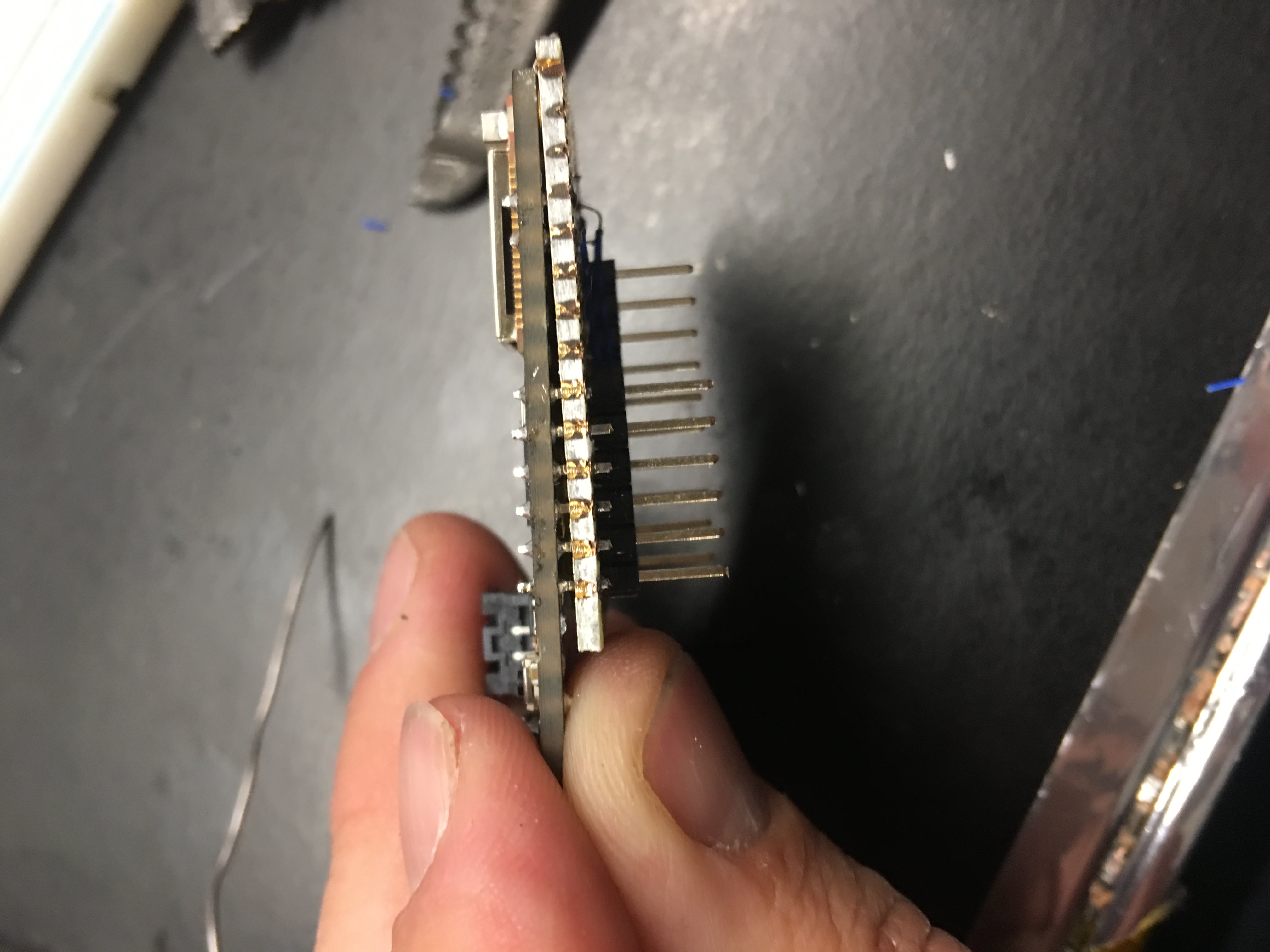 Side view of the adapter with the feather. Overall the assembly adds about 1/4” to the keyboard’s height.
 Close up of the completed assembly. You can see the switch, which is just glued to the switch plate, and the various connectors.
 Wider view of the completed board. I’m using some M3 standoffs to give me the required height.
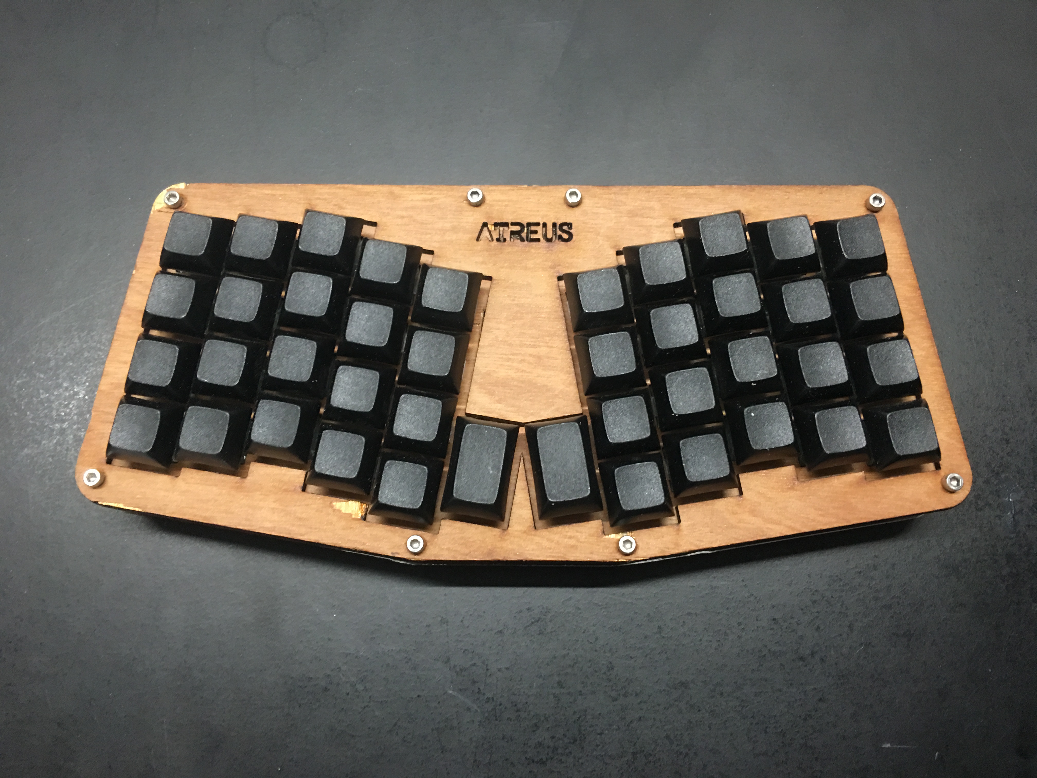 The top of the completed keyboard. It’s somewhat battered, and I may do another when I get my laser cutter up and running (parts inbound), but that’s yet another post.
-
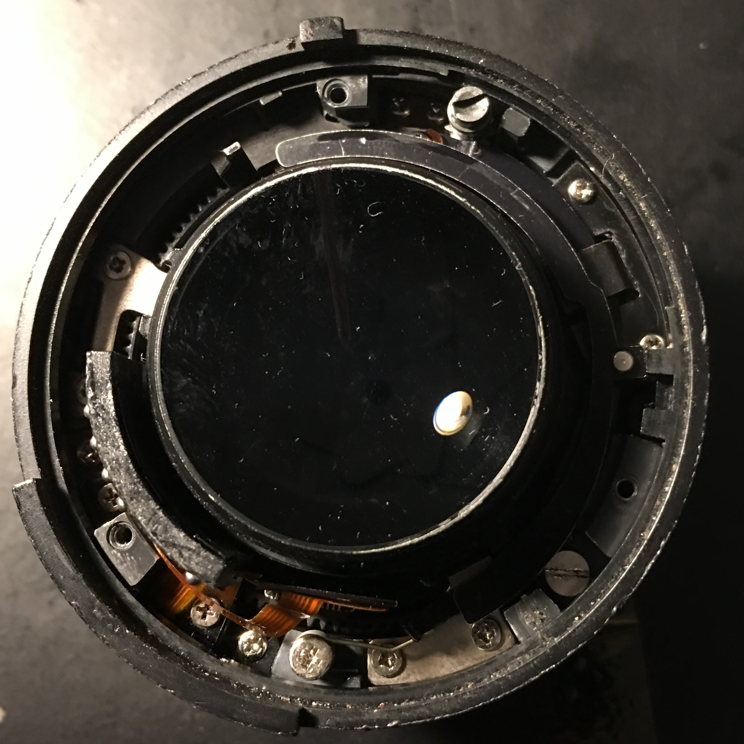
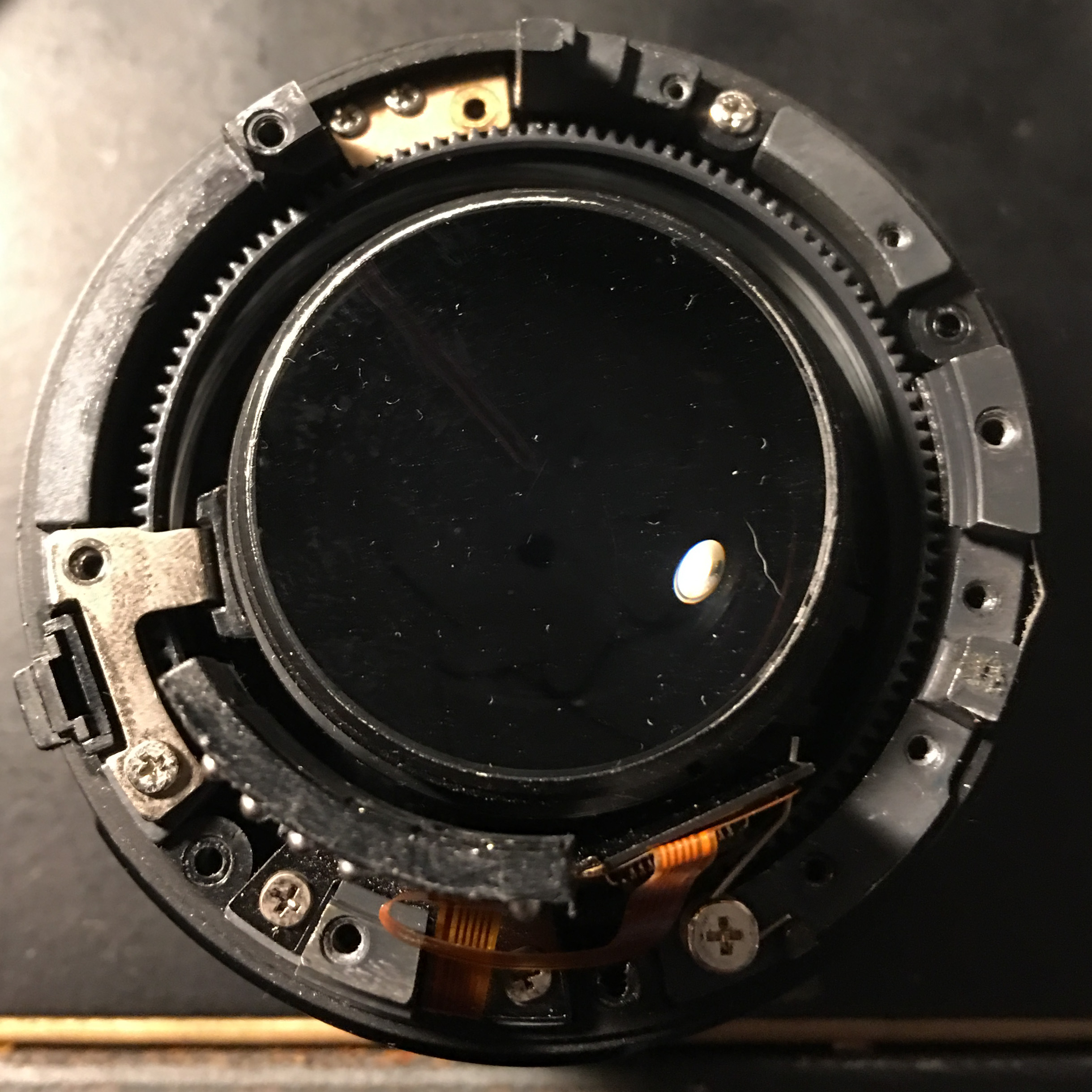
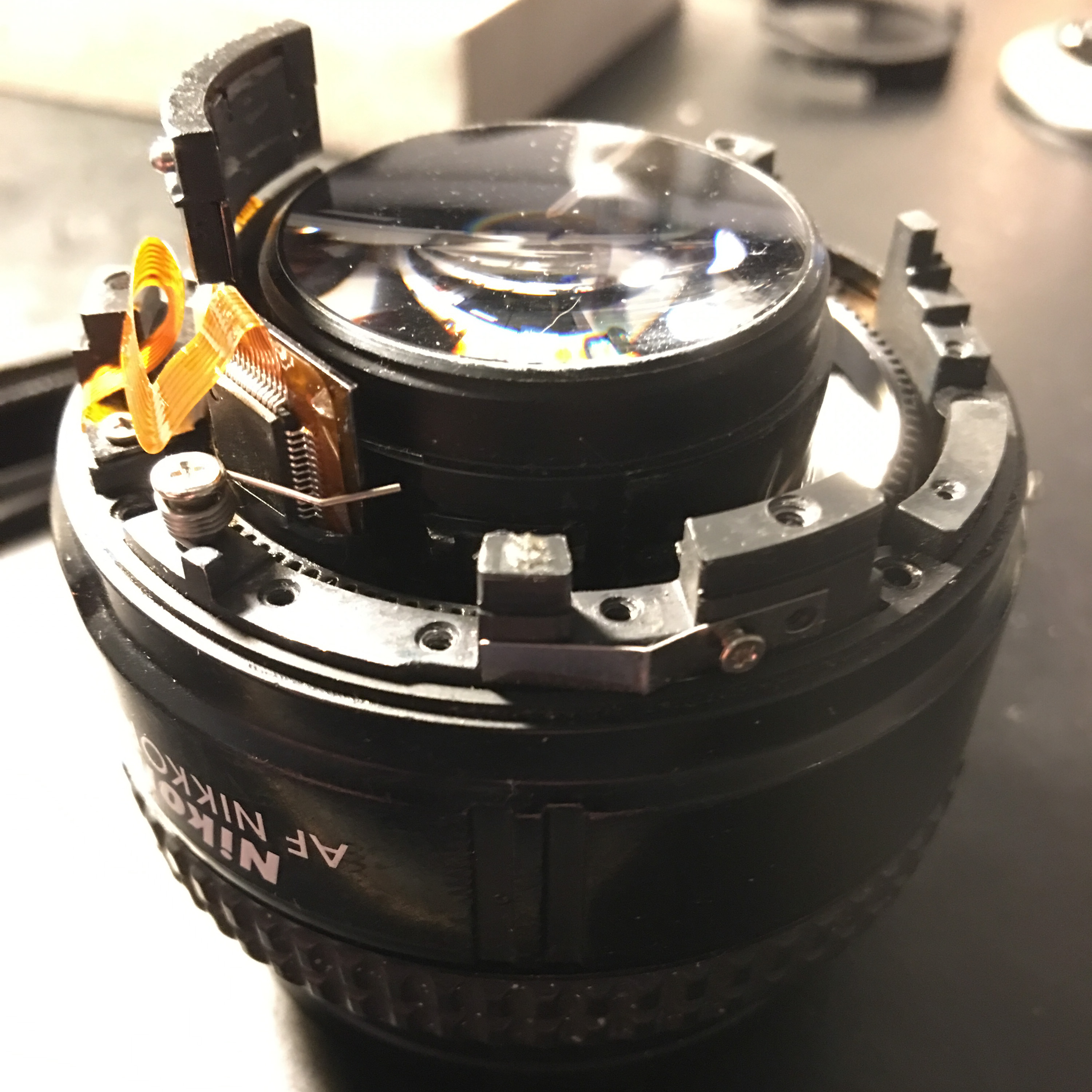
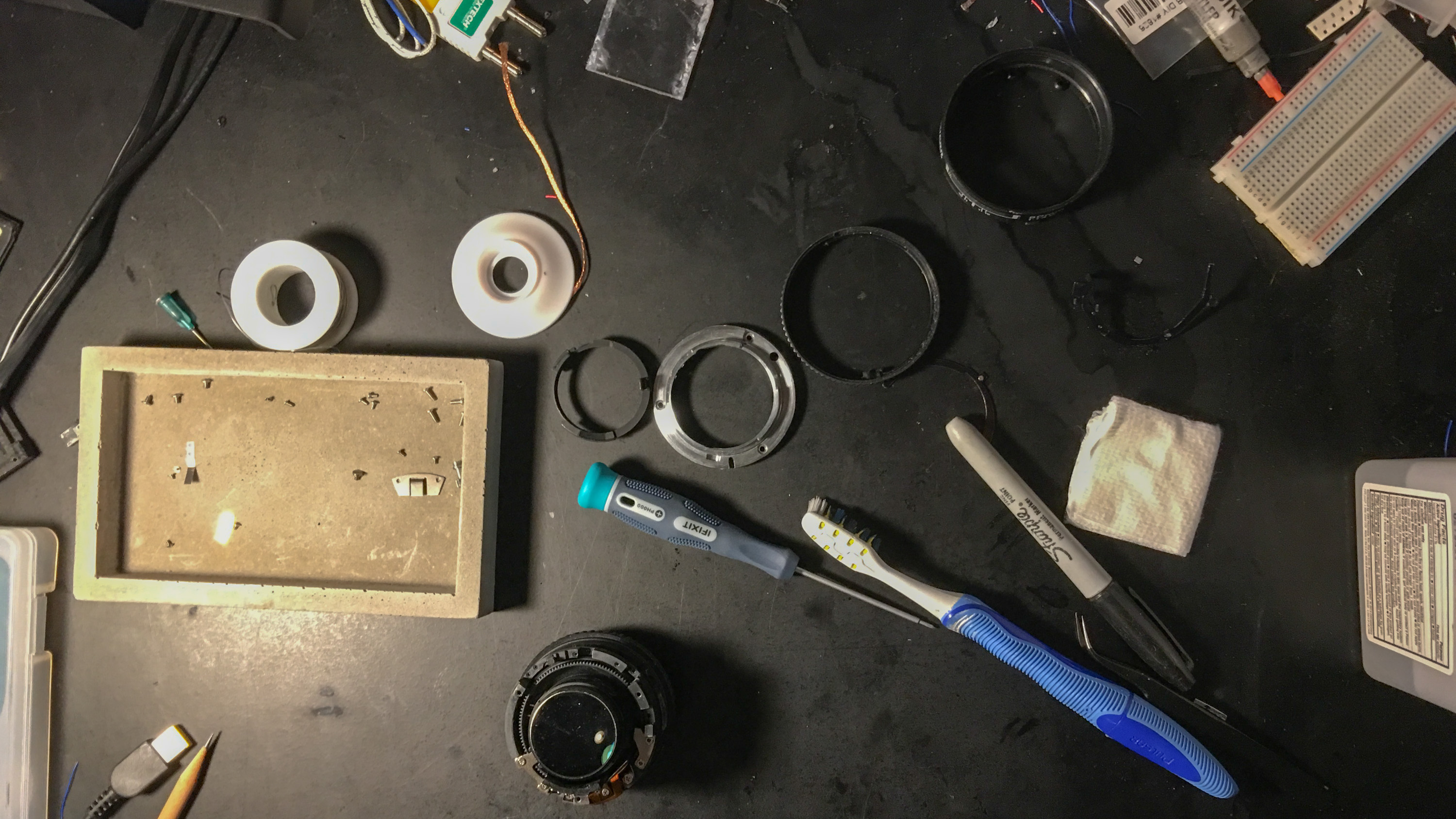
notes on disassembling an SLR lens
So, this isn’t a detailed teardown of this lens; if you want that, maybe hit me up and I’ll give you a blow-by-blow over some beers. This is a general set of guidelines for doing dissassembly of something complex that you need to do something to, but don’t really know how it should be assembled. For anyting other than a lens, just substitute it in; I use the same techniques on laptops or computers or telescopes or whatever.
Firstly, I’ll pass on a tip I read somewhere when I was about half the age I am now: when disassembling, imagine the machine is a bomb, and if you pull too hard or force something it will go off. The metaphor extends: the bomb will blow a hole in your bank account.
So: what will you need? First: the right screwdriver, wrench, pin-spanner, or other tool as required. For this job, it was an assortment of 000 and 00 philips head screwdrivers. Disassembly of lenses requires the right tools. You can make the attempt without the tools, but it most often ends in damaging something; I have a 50mm 1.2 Canon (in Leica thread mount) with a damaged rear element to testify to this fact.
Second: calm. A person or people designed the lens; you’re also a person, and you’re capable, with a little thought, of understanding the design, at least of the mechanical parts. Further, the assembly of the lens was left to people on an assembly line in a factory, so it shouldn’t be rocket science to take it apart and put it back together. It helps to be able to stop the work when you’re tired, and come back fresh later.
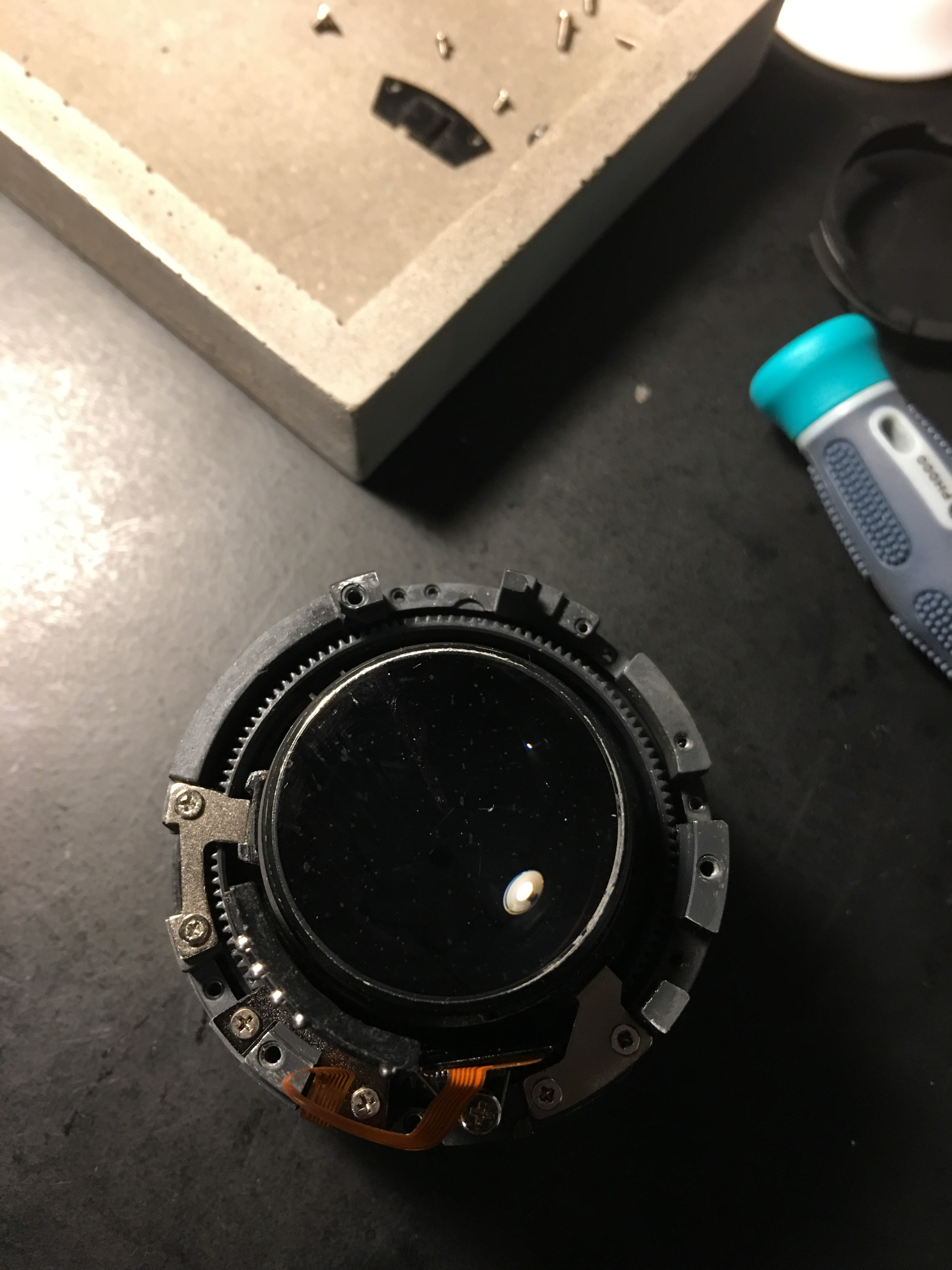
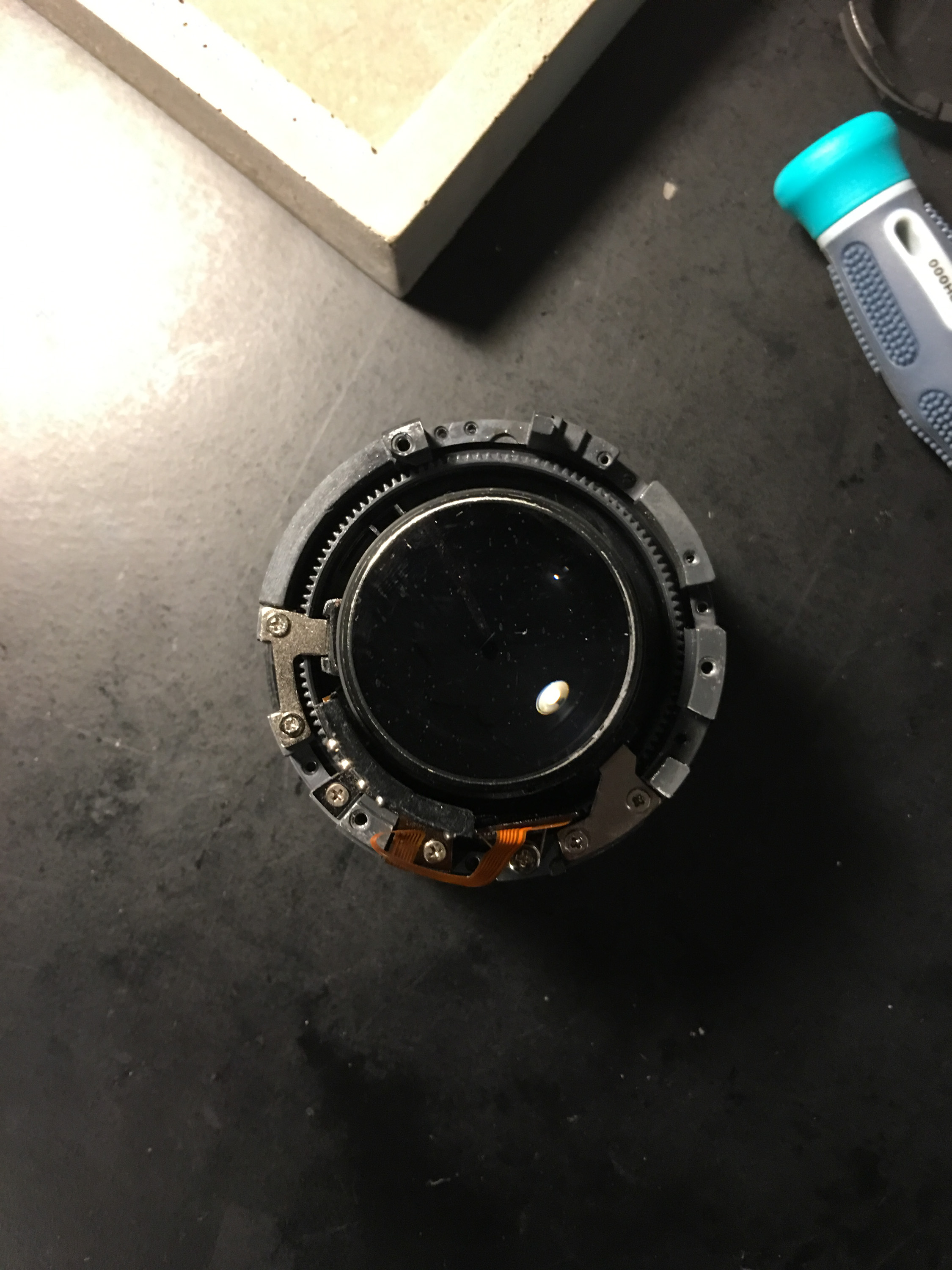
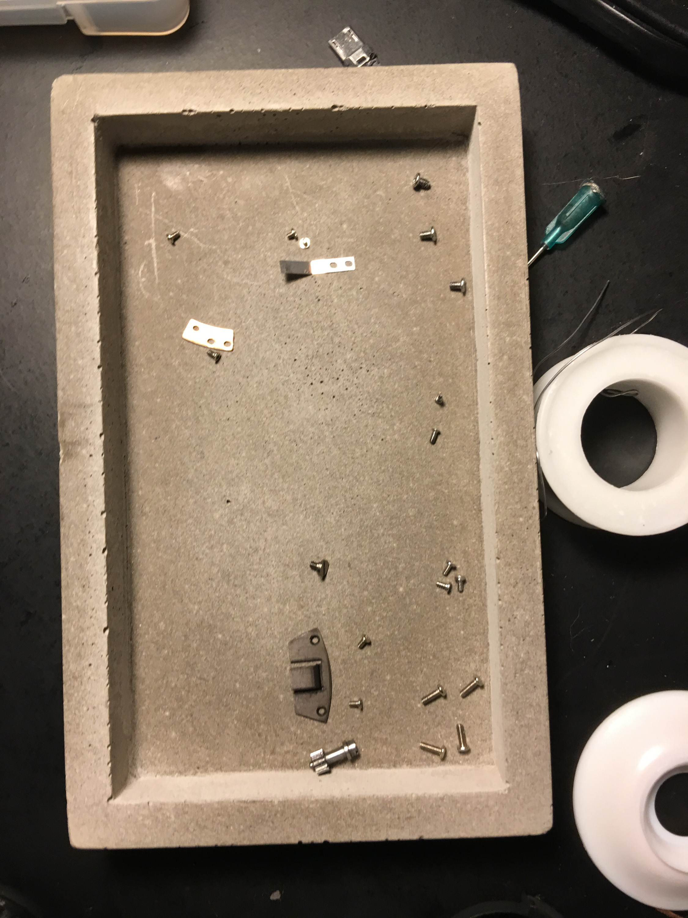
So, to help facilitate that, I do a couple of things. I take pictures as I go, just on my phone camera, to help me note the orientation of parts and screws, and to remember the order that things came apart in. Sometimes one or two pictures is sufficient; sometimes, like this repair, I’ll take pictures of every part as they come off. (I’m not showing all of them, because that would be pretty boring).
I have a screw tray, usually just some container that also happened to be on my desk, to put the screws in as they come out. The gray one you see here is concrete, part of a desk set I got and didn’t know what to do with. Small parts also go here, since they are just as easy to lose.
The large parts just get knolled into rows as they come off, since they’re harder to lose. I actually stopped this repair in the middle, had dinner, watched some TV, and then went back to it, knowing all the things I needed to know to finish it were there.
Once the lens is apart, you can do whatever repair brought you here in the first place. In my case, the helicoids had gotten dirty over years of use, and I needed to clean them. I used isopropyl alcohol, a toothbrush, and paper towels for cleanup. It’s not the strongest degreaser, but half of the threads were plastic, and I didn’t want to chance melting them. Instead of grease, I wiped on some machine oil, and began reassembly.
Often the hardest part of lens repair is reassembly. Getting the helicoids mated properly (with the correct rotation) I always find really difficult, and a matter of trial and error. Once that’s done, the rest I find pretty easy, just a matter of getting the right screws in the right places.
Some other notes: Ribbon cables are especially delicate, and nearly impossible to repair. Do everything in your power to avoid pulling on them or bending them too much. If the optics in the lens aren’t a sealed unit aligned at the factory, make a note of the number of turns you make getting it apart; this may help with alignment (but if you’re trying to align lens elements, you’ve gone beyond the scope of this guide).
Good luck and happy hacking!
-
senoko pt 2 and other notes on higonokami bringup
So, over the last couple weeks, I’ve been making progress on the new laptop, which I’ve been calling ‘higonokami’, after the Japanese style of pocket knives. I have this thing for naming my laptops after simple machines. Anyway, progress has been steady.
First, building the senoko. I recieved my boards from OSHpark and they were great. I still have two extras and no idea what to do with them. The stencils I ordered at first were for the wrong version of the board, so I had to re-order them. It was just as well that I was delayed a couple days, until the weekend. I started working on the board at around 9pm saturday and took it out of the oven at 2am sunday. It programmed immediately but there were a few solder bridges I didn’t catch that caused it not to work right away.
Before I get too far into the bringup, I’d like to diverge into talking about placing all those components by hand, which took most of 4 hours. I was working from the BOM and trying to place all the components of one type at once; all the 100k resistors, all the FETs, etc. About halfway through, I realized it would have been quicker to organize all the parts first, and then go over the board in one pass and place them by reference as I found them. I got it done, anyway.
So, back to the bringup. I got it programmed, and then had what I thought were issues with the gas gauge. As it turns out, it just takes a little time to settle down. But, I decided I’d replace the one on the board with a spare, and try that. After that had the same issues, I started messing with the battery connector, and ended up shorting it, damaging the gas gauge and a current sense resistor. I thought it was just the gas gauge, since it started showing new worse symptoms, so I ordered a couple more and didn’t work on it for a week while I waited for parts.
When the new chips came in, I got one installed with my reflow setup (hot air is an essential tool), and saw it having the same issues. So, I went to the schematic, and stared at it for a while. I saw that maybe the current sense resistor had something to do with something, so I tried shorting it, and suddenly the GG came to life. A few minutes and a spare resistor later, it was working fine, and the battery was charging. Shortly after that, I was able to unplug it from the AC adapter, and confirm everything was working.
So, with that done, I’ve been focusing my efforts in two areas: getting the software setup reasonably squared away, and getting an adapter made for the LCD I’m using. The board I’ve made is just a passthrough to adapt one cable type to another. I’m using a comercial board with the same chip as the eDP adapter that came with the novena kits.
The software has been a little more complicated. This is an ARM laptop, armhf arch. There are some things precompiled, for example Chromium is available pretty easily, but Atom is not, and some other creature comforts aren’t here. There’s no onepassword port, even to Linux. Most of the debs I’ve been getting from the ubuntu 14.04 repos. Also, there’s no lightroom equivalent, so I may have to get creative.
In near future: a sheet metal case for this beast, clamshell, just like any other laptop. Friction hinges from McMaster Carr make that possible. Also, the LCD bringup is soon. That’ll pretty much finish this off. I’d like to have it done in time for our trip to oklahoma. We’ll see if that actually happens.
-
building the senoko power board
TL;DR – board is shared on OSHPark here, BOM is at mouser here, and stencils from OSHstencils
(you should be able to export the cream layers from the KiCAD versions of the board [here](//bunniefoo.com/novena/novena-accessories-kicad.zip))CORRECTION: get the PVT gerbers here and use the.gtpfile.So, my laptop died over the weekend, not permanently, but enough to get me thinking. The failure was in a tiny component that I could probably fix, if I knew what it was and could source it. This got me thinking about the Novena, which is a completely open source laptop, built to be as open as possible. It’s not a fast machine, but for most of my uses I really only need a typewriter with some sort of UNIX-like environment, usually debian or ubuntu. So, somewhat spurred on by the ennui of a broken machine, I ordered a board.
The first problem with this scenario is that the battery board, Senoko, the thing that handles charging and power management, is not available. Since it’s open source, that’s fixable.
The board is only four layers, so we can have it made by OSHPark. I downloaded the gerbers from the site, and uploaded the file directly. I chose OSHPark because I’ve used them in the past, and DirtyPCBs’ 4-layer non-custom size is 2cm too small in one dimension. There are two plated slot holes, which OSHPark doesn’t support, but they’re mounting tabs that can be cut to fit the round holes. The rest of the board is standard, and doesn’t present any issues.
The second part, ordering the BOM, is a little trickier. Most of the components are cheap, and so we get enough to get at least the 10 item discount. Some things, I only ordered 1 of; if you want to make two boards, it’ll cost an extra $30 or so at this step (only double the components that aren’t already doubled because of quantity discounts), and double the time at assembly. There are a few substitutions from the original BOM: both of the ferrites were EOL’d, so I found equivalents for them. The barrel jack connector isn’t identical, but the closest mouser had, and should work. One of the fuses wasn’t available, but a close equivalent was. Finally, the supercap was also EOL’d, so it’s replaced with a similar one (slightly more capacitance, but it should work, since it’s a power storage device in this circuit).
The stencils are another thing.
You'll need to open the board in KiCAD or Altium (if you have altium and know how to use it, you know how this works). Then go to File->Plot, and select the two cream layers, and then export them.Correction: Download the PVT gerbers here and use the.gtpfile for the top layer, and thegbpfor the bottom layer, if you want it. I decided I didn’t need it for a dozen passives. Go to OSHstencils, follow the directions to upload the files, and order them.Board assembly is, at this time, an exercise for the reader. There are plenty of good tutorials out there if you haven’t ever done surface mount work before. None of this is too terrible; as long as you get the components roughly on the pads, the surface tension of the molten solder will move them into place. The only real hair-shirt part of this project will be hand-placing 226 components with tweezers; it’s a lot to place by hand. The board is small enough that you can get it in a toaster oven for reflow, and there are few enough components on the bottom that they can be hand soldered. I’ll probably use hot air for the bottom, just to save myself trouble.
So, that’s it. $220 worth of material and you can put it together, assuming you have access to a reflow oven, solder paste, and the sundry tools needed. Probably the MVP for that is a halogen work light and Chip-quik low temp solder paste. Lovely stuff, but beyond the scope of this post. Go forth and google.
-
situated systems open house on pier 9
This was an event I went to looking for ideas to steal. Since I didn’t go as a reporter, didn’t have my ‘must get everything down’ hat on, this is more a disconnected set of notes than a useful story. The idea for the project was to give four brilliant academics from diverse fields free reign to do research, and see what they come up with. They decided to focus on the ways the military industrial complex had affected the Bay area. In their own words:
… Situated Systems, an experimental, collaborative, site-specific research project which explores military and industrial infrastructure in San Francisco and the Bay Area, investigating how this history has shaped the technology culture of the region and its outputs.
(found here)
Deb Chandra summarized it in four words: Atemporality, Illegibility, Visibility, and Materiality. The idea that appealed to me most was that of materiality, that “As soon as you instantiate objects, they start to interact with the environment they’re in,” as my notes say; pretty sure that was a quote from Chandra’s presentation.
I love the idea that the things that happen leave traces; sometimes it’s a crane, but more often than not it’s a superfund site. One of the outputs was a map which talks a lot about where these things are, and some of the history. There were also a lot of hand-held pieces at the show, with more extensive research than is in the map captions. All interesting, even if some of it I already knew.
So, the setup: a 20x40 white box of a room, projector on one wall, and several tables around the room, up against the walls, with different bits of art on them. There were also photos, printed on canvas, hung above the tables. About 30 chairs took up the center of the room, for people to sit during the talks.
The first table I looked at was zine printed with a laser cutter on plywood. It was meant to be housed in a heavy welded steel box. Nice welds. Of course, at this point I wasn’t thinking of a write up or even really thinking at all, so I don’t have any pictures of them (I am a terrible reporter, but in my defense, I was also super awkward, having not been at an event like this ever before). There was a sign on the table, encouraging people to handle the objects.
The next table had several 3d-printed models of large machine tools, along with little workers, standing at them for scale. Again, I super wish I had gotten photos of them; again, I’m a terrible correspondent. In the moment, I was much more interested in the people around, but also super bad at introducing myself.
I didn’t get a feeling of value judgements coming from the work, but rather a recognition that history is complex. The presentation of facts seemed to be equal parts wonder (the old tools, the Bay Model, etc.) and horror (number of superfund sites we’ve created in a population center). It’s equally possible that I’m not familiar with the context, and getting it wrong. But, there was this interesting meta-idea that I took from a conversation with Deb Chandra: that this work gives greater context to the places I see all the time. The building we were in, Pier 9, used to be a military installation. When you look across the water from there, you can see Treasure Island and Alameda, both decommissioned, both poisoned. But you’re also in a place that couldn’t exist without all that activity to support technological growth.
A series of disconnected notes:
To read:
- Situated Knowledges (Haraway) – referred to as one of their ‘patron saints’. I was only dimly aware of her work previously.
- All of their zines – there are only two up currently, but they did four. I assume they’ll upload pdfs eventually.
- Their bibliography – They’re a bunch of academics, of course they did up a bibliography. You could do worse than work down their list of reading.
- Tinyletter – where I presume they’ll be sending out info as more stuff comes online.
Also, they’ve given me a list of places to visit: (if any of my bay area friends want to field trip, get @ me):
Look, just anywhere on their delightful map.
-
some notes towards a MF scanner camera
So, one of my great ambitions in life is to make a digital camera. I’ve made several attempts in the past, but none of them have gotten past the “yes, that’s physically possible” stage. There have been some recent developments worth sharing, though.
First, there’s the Aptus who are building a cinema camera from scratch. It’s a small team, and they’ve built several prototypes. What’s that, you say? They’re professionals with vastly more experience in the area than me or most amateurs? Yes, but it’s all open source, so we can look at those designs, and at least learn from them what kind of components they’re using, how they’re dealing with timing issues, and learn the vocabulary of camera building. Never underestimate the power of knowing the right word; at least, then you’ll know what to google.
Then there’s TinyMOS which I thought was open souce, but isn’t. Still, it’s three guys, knocking together a camera. Impressive, but it gives me some idea of the scope of the project; one guy, working for a reasonable amount of time, can find some success.
Then, there’s this linear CCD module on hackaday. For our purposes, it’s a working single pixel wide camera. All of the parts can be had for $50 in single quantities, which is unheard of. Any other single row detector that I can find is in the hundreds to thousands of dollars, and that’s without support equipment. So, how do you turn a single strip of pixels into an image? You move the strip, of course. There was a class of back (may still be) for medium and large format early on in the digital era known as scanning backs, so called because they scanned across the film plane. Now, if I’m reading the spec sheet right, the minimum shutter speed for the TCD1304 would be something like a minute to scan across a medium format piece of film. Read, move the sensor 8 microns, read again. You’d need a slit 8 microns across, as well, to mask off the 200 micron (0.2mm) wide pixels, but that’s doable.
A crazy thought just occurred to me. The sensor is ~1cm wide, and cheap. Four of them could fit, side-by-side, and you could divide the movement and the time to record by 4 as well. Alignment would be a bastard. But it’s just within the realm of possibility. A fifteen second readout would be a lot nicer than a 60 second one.
I’ve been sitting here for 10 minutes trying to figure out if there are linear actuators that can handle that fine of movement for reasonable prices, and then I saw that the wikipedia for linear actuators has a DVD player. The head movement is in the range of what we need. Track width on a dvd is 1.1µm, and our pixels are 8µm. So that’s fairly possible.
So: several days later, I’m coming back to this, and I’ve ordered a Mamiya RB67 with several lenses and two backs. I need to order all the parts for the CCD, but first I have to put together a bill of materials. Said BoM will have to include a DVD drive, all the parts from the hackaday post, some 3d-printed adapters, and probably some linear bearings. I’m calling it now: first light before my birthday (in September 😉).
-
tv blinders
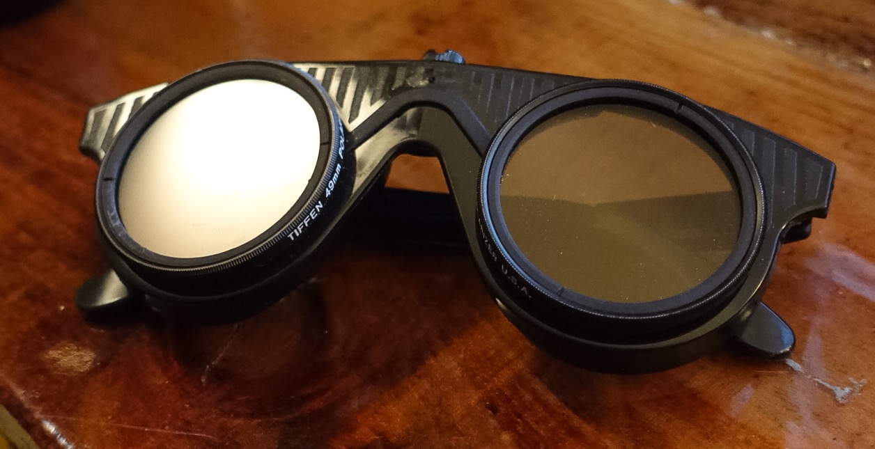
Like all my hacks, these start with a problem. I got a new job. That’s not the problem; don’t rush me. I got this job, and my work is all about concentration. At this new job, there are TVs all over the place, with sports playing. Televisions are infinitely distracting. So, naturally, I tried to come up with a technical solution. First, I thought about using a TV-B-Gone remote, and even bought one (that name is trademarked, hence the less catchy title of this post). However, other folks in the office like having them on, and some even need them to do their jobs. So, I needed to block it, but only for myself.
Then, I had a little luck. In the office, there are some 3d screens, with glasses. I was waiting on a meeting, and put on the glasses, and looked at a normal screen, and saw that out of the 3d glasses, one eye couldn’t see the normal screen at all. This connected with a memory of 2d glasses, which are for viewing 3d movies without the 3d (handy for folks who get motion sick, or are annoyed by gimmicks). In a regular TV (these days), the light is all polarized one direction; for a 3d screen, one eye is polarized one way, ant the other perpendicular. All I had to do was take a linear polarizer, rotate it the right way, and keep it between my eyes and the television.
So, armed with the knowledge that the right angle of polarizing film blocks the light from the TV, I made the first version. Cheap fashion glasses and polarizing film. Pop out the lenses that came with the glasses, then hold the film up to a television and turn it until the tv goes dark. Mark that orientation, and cut out lens shapes. Put these in the grooves in the glasses, and it should work. If they don’t fit, you can trim them until they do.

As you can see from the picture above, they worked, but they were pretty wobbly; the film had to be cut just so to stay in the grooves of the glasses. So, I made another version. I knew from previous experience that welding/cutting goggles were great for this sort of thing; flat, round lenses that are made to be interchangeable. And, because of my photography, I knew that linear polarizers come in the right size. So I got these glasses and two of these filters. Take the super dark lenses that came with the glasses out and put the filters in, so that the frames grip the filter threads. These filters are made to spin freely, so they can be oriented.
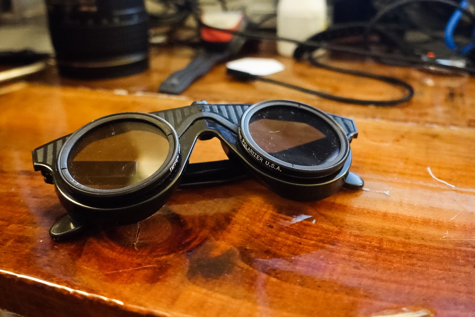
To use the glasses, simply put them on, look at the television, and turn them until the picture is darkest.
-
first hack: battery-less magic trackpad
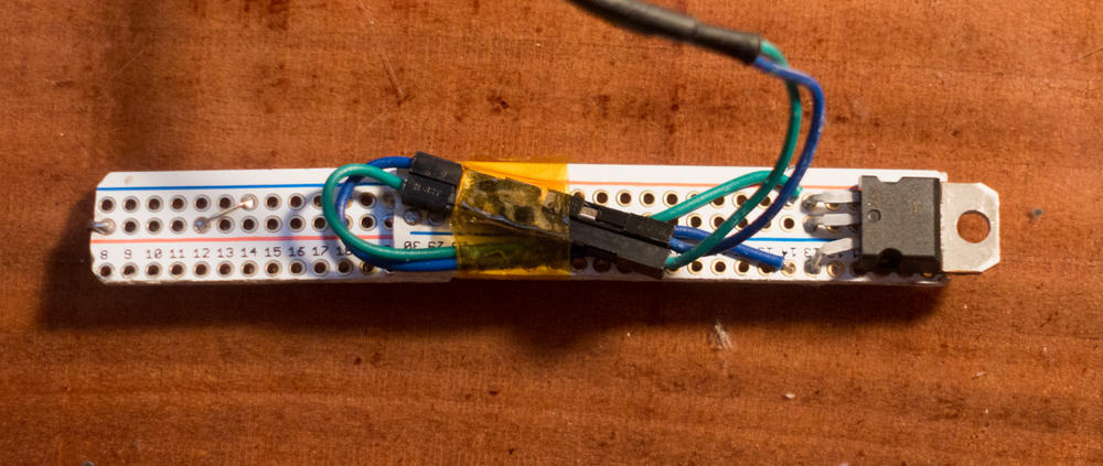
This hack is something I’ve been meaning to do for a while, but only realized today I had all of the parts. The problem is I really like my magic trackpad, but I hate wasting batteries on it. It’s forever tethered to my desk, about six inches from all the power you could want coming out of USB ports. There are a couple problems. First, the trackpad has no input for power other than batteries. Also, The USB ports output 5v, and we need ~3v.
So, what’s a hacker to do? Build an adapter, of course. To do that, we’re going to need some supplies and tools.
-
A linear voltage regulator: https://www.adafruit.com/products/2165. This is one I had on hand. It turns 4-16v to a clean 3.3v, close enough for our purposes.
-
Perf board: https://www.adafruit.com/products/1609 . I like these because they have a power rail running down both sides.
-
Connectors. I used some male to female jumper wires I had in the junk drawer. That said, you could cut one of these in half: https://www.adafruit.com/products/1131 and use it for a more compact fit, if you don’t have stuff lying around.
-
Heat shrink tubing or electrical tape. Heat shrink is a lot neater: https://www.adafruit.com/products/344
-
USB cable.
-
Soldering iron, solder. If you’ve never soldered before, this isn’t the project to start on. We’re making structural joints as well as electrical.
-
Drill and bit: I think I used a 3/16th inch, use your judgement; it’ll need to be big enough to fit your connector through.
-
Board cutting implement: I used a pair of tin snips, but a Dremel would work as well, they’re just louder.
Now that you have all of your supplies, assembly is pretty easy.
-
Cut the power strips off of the perma proto, leaving one row of extra holes on each side (as pictured).
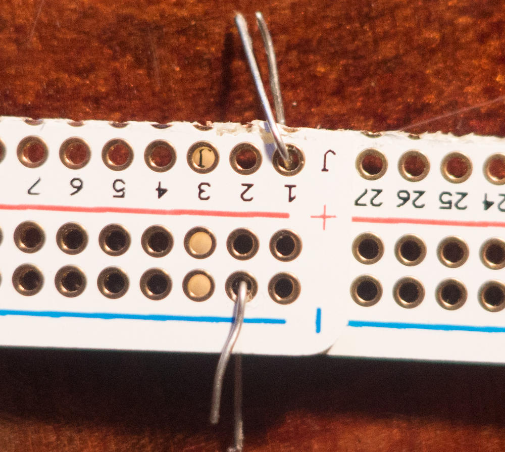
-
Overlap two rows, so that you have six holes lined up in both boards. Above, I’ve used a couple bits of wire to hold them in place. Then, fill all of the overlapping holes with solder.
-
Now that the boards are attached, you can solder the regulator. The middle pin is Vcc, and looking at the top of the regulator (with the part numbers), Vin is on the right (bottom, in the picture of the completed adapter), and Ground is on the left (top, in the picture). I put Vin in the non-bus holes, because it only has to be connected to the usb. You want it to stick over the end a bit. The tab on top is also connected to Vcc, and will serve as the positive terminal.
-
Connect your connector to the board, in a way you can remember. For mine, green is ground. Then, cut and strip off the small end of the USB cable, and connect it to the other side of your connector. Red is Vin, and black will be ground. You can trim back the green and white wires, you won’t need them. If you have some heat shrink, remember to put it on before you splice. Solder and insulate the connections, in any case. This guide is a good one to look at to know if your splices are up to snuff.
-
If you have a multimeter, plug everything in and check; you should have about 3.3v between Vcc (Vout, on the datasheet for the regulator).
-
Trim the board to length. You need to be fairly accurate, but you can add a metal spacer if it’s too short.
-
Then, wrap a bare wire around the edge, so that it sticks out of the center. You want it to make contact with the end of the battery compartment. Connect this with ground. Check for shorts before you plug it in again; we don’t want to let the magic smoke out.
-
Remove any batteries that are in the trackpad (duh). Drill a hole in the on the back of the battery compartment. (see pictures) De-burr with a larger drill bit if you have one, but don’t fuss too much, it’s purely cosmetic.

-
Disconnect the USB cable and feed the connector through the hole. Hook it to the board connector, and then gently feed the whole assembly into the battery compartment. Screw in the cap, and connect the cable to power. You should be able to turn the trackpad on.
That’s it! It’s a lot of words for what was about 45 minutes of work. The sharp eyed reader may have noticed the jumper on mine; on the other side of the board, I’ve cut the traces, and moved ground over to the center, for a better position on the end connector.
-
-
New blog, new hacks
So, this is my new tech blog. I decided I needed a little more room to move than the project specific watch blog, so here we are. A real post is coming, right after this.