iphone x
I just read the iFixit teardown of the new iPhone. The new phone is a remarkable piece of technology but I’d like to draw your attention to one image in that post:
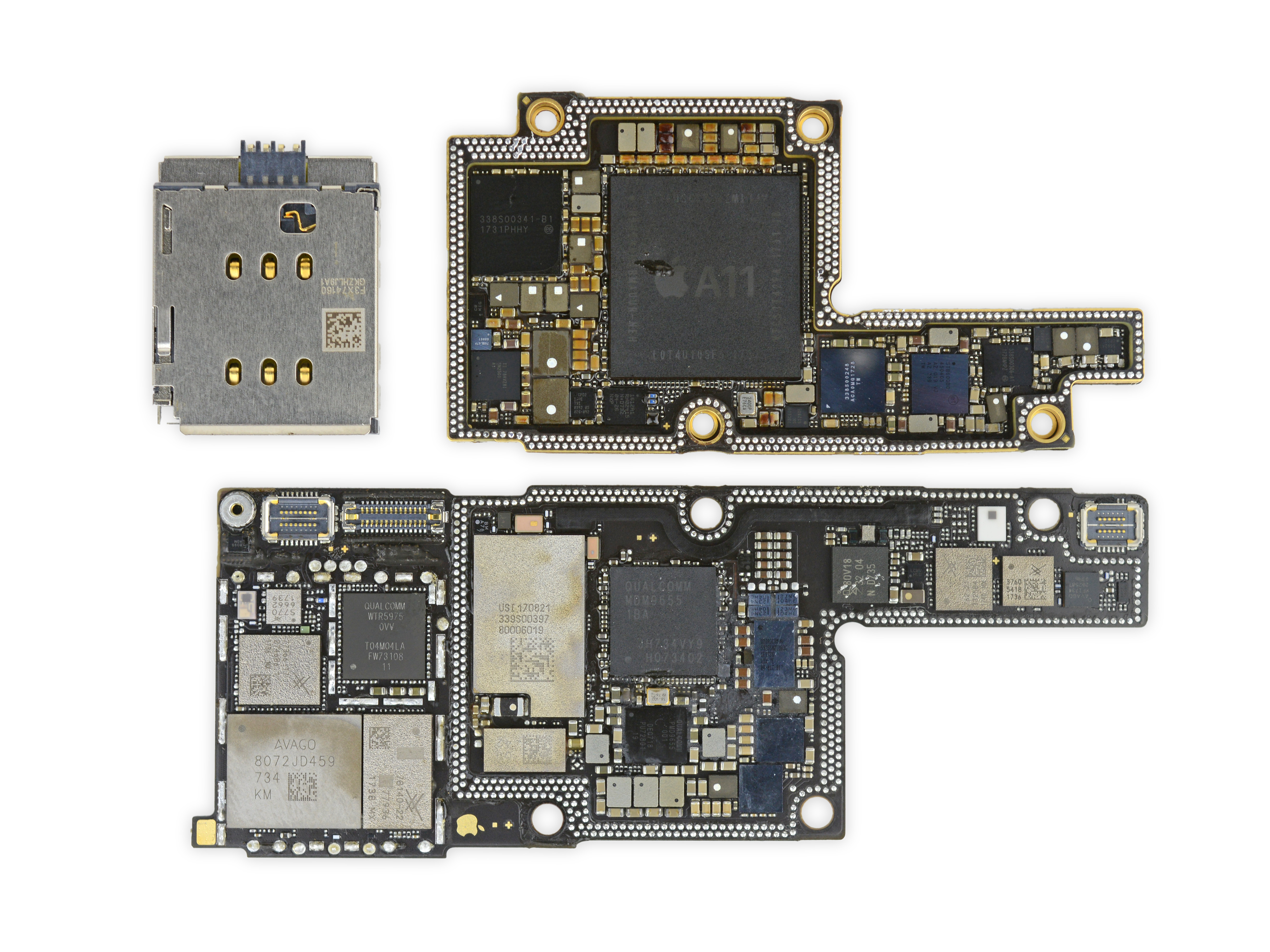
Now, to most of you I’m sure this looks like a bunch of blobs and glitter, separated by large rectangles. It’s really a lot more than that though, and I’d like to talk about what I see when I look at this photo.
It’s a product shot, evenly lit, on a bright white background. The product stands in stark contrast to the cleanness of the surface it’s shot on. But other than that, it’s not much to write home about, aesthetically.
This picture is all about details, though. The surfaces of both sides of the interior of this PCB sandwich are a perfect horror vacui; every available space is covered. That means that almost none of the area on the top of the board is given over to traces, the lines on the board that actually connect the part; it also means there are a large number of blind and buried vias, which are both more expensive and error prone. I see this and I think, that’s gotta be at least an 8 layer board on each side.
Then I start to think about how I would design this. The upper bound for the number of traces, every pin discreetly connected to every other pin, is on the order of millions of them, but I’d be surprised if there were more than 10,000 “nets” (that is, discreet connections between sets of pins). For reference, my watch has 100, and took me a week to route. The engineers that built this board could do mine in an hour or two, probably; so we’re talking 1,000 engineer-hours just to route the connections on the boards. That’s one guy and 6 months, or a team of 10 (with managers) and 2 months (because engineering time doesn’t scale lineraly; coordination of effort takes time, too).
It’s probably a team of 20 and consistent 1 month iterations; they have to do quick turns for problems and changes in the supply chain, uncertainty about whatever parts come in, alternate versions for different vendors for different parts (different cellular radios, sensors, whatever). There’s a lot of uncertainty when you begin a project like this. You don’t know what the vendors can really deliver in 18 months in quantity 100 million. That’s not 20 engineers total, but 20 for this small facet of the overall design.
For example, the cameras. The cameras, even one of them but especially both of them, represent an amazing amount of work. The sensors had to go through design and testing; the optical systems, likewise. They have autofocus and optical image stabilization, which is completely nuts. Not just “man this is a lot of engineering” but “are we sure apple isn’t working with aliens on this one?” nuts. (It’s really just the progression of a bunch of related tech, including accelerometers and very small electromagnets, but I digress).
Even once you have that design, it’s not done; there are assembly and process engineers that have to do their work, too. The robots that place components work a certain way, and the tool paths that put the components in place have to be right, or there’ll be too many failures.
There are a couple other interesting facts I’ve gleaned from this picture: they’re using what look like chip antennas for bluetooth and WiFi, which is a little odd. I could be wrong about what those pink blobs are, though; usually the antenna is part of the metal bezel on the outside of the case (those may be test antennas or something, too). There’s the crazy notch in what turns out to be the bt/wifi chip to accommodate a big capacitor (first spotted on twitter by someone else). That either means the supplier put that there and they’re taking advantage of the board area, or apple asked them to make that notch. Nuts.
So, yeah. I might have to pick one up.